Large-area perovskite light-emitting film and light-emitting diode thereof

A technology of light-emitting diodes and light-emitting films, which is applied in the manufacture of electrical components, electric solid-state devices, semiconductor/solid-state devices, etc., can solve the problems of non-dense perovskite light-emitting films, high solution waste rate, low light-emitting efficiency, etc. Dense, smooth surface and uniform luminous intensity

Pending Publication Date: 2021-12-03
JINAN UNIVERSITY
View PDF0 Cites 2 Cited by
  • Summary
  • Abstract
  • Description
  • Claims
  • Application Information

AI Technical Summary

Problems solved by technology

[0004] In order to overcome the deficiencies and shortcomings of the prior art, the primary purpose of the present invention is to provide a large-area perovskite luminescent film, which solves the problems of non-dense, uneven thickness, low luminous efficiency and The problem of high solution waste rate

Method used


Image

  • Large-area perovskite light-emitting film and light-emitting diode thereof
  • Large-area perovskite light-emitting film and light-emitting diode thereof
  • Large-area perovskite light-emitting film and light-emitting diode thereof

Examples


Embodiment 1

[0047] Preparation of PEABr:CsPbBr with different molar ratios 3 Large-area perovskite thin films:

[0048] (1) Preparation of perovskite precursor solution:

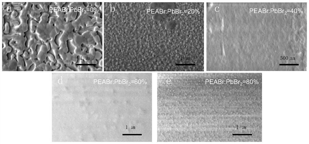
[0049] CsBr and PbBr 2 Soluble in the organic solvent of DMSO in equimolar ratio (CsBr=0.3M, PbBr 2 =0.3M), after mixing evenly, it was divided into five bottles of 1mL solution to prepare a 0.3M perovskite solution. Then add relative CsPbBr to these five bottles of solution 3 Solution molar ratio is 0%, 20%, 40%, 60% and 80% PEABr, obtains the (PEA) containing different molar ratio m (Cs) n-1 Pb n Br 3n+1 Precursor solution of type perovskite.

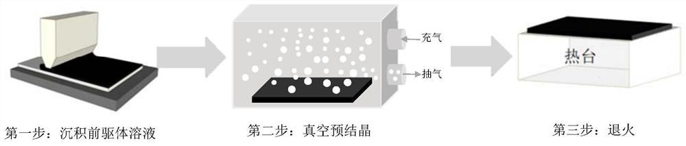
[0050] (2) (PEA) with different n values m (Cs) n-1 Pb n Br 3n+1 The preparation of large-area perovskite thin films of type perovskite is as follows figure 1 Shown:

[0051] In a glove box at a room temperature of 19°C, set the height difference between the scraper and the substrate to 220 μm, drop a volume of 26 μL of the perovskite precursor solution onto the g...

Embodiment 2

[0053] (1) Preparation of perovskite precursor solution:

[0054] 0.5mol CsBr and 0.5mol PbBr 2 Dissolve in DMSO organic solvent, mix well and then add relative to PbBr 2 40% molar ratio of PEABr yields (PEA) with an n value of 5 2 (Cs) 4 Pb 5 Br 16 Precursor solution of type perovskite.

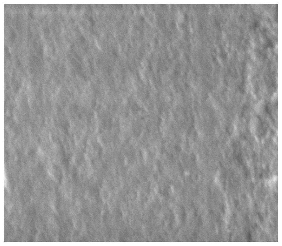
[0055] (2) (PEA) with an n value of 5 2 (Cs) 4 Pb 5 Br 16 The method of preparing large-area perovskite thin films is as described in Example 1: the morphology of the perovskite thin films is as follows image 3 As shown, the thin film is dense, uniform and has high photoluminescence efficiency. Its photoluminescence efficiency is as Figure 7 Shown as high as 32.3%.

Embodiment 3

[0064] Preparation of PEABr:FAPbBr with different molar ratios 3 Large-area perovskite thin films:

[0065] (1) Preparation of perovskite precursor solution:

[0066] FABr and PbBr 2 Soluble in NMP organic solvent in equimolar ratio (CsBr=0.4M, PbBr 2 =0.4M), after mixing evenly, it was divided into five bottles of 1mL solution to prepare a 0.5M perovskite solution. Add relative FAPbBr to these five bottles of solution 3 Solutions with molar ratios of 0%, 20%, 40%, 60% and 80% PEABr obtained different n values ​​of (PEA) m (FA) n-1 Pb n Br 3n+1 Precursor solution of type perovskite.

[0067] (2) (PEA) with different n values m (FA) n-1 Pb n Br 3n+1 The large-area perovskite thin film is prepared, and the preparation method is as described in Example 1.


PUM


Abstract

The invention discloses a large-area perovskite light-emitting film and a light-emitting diode thereof. The large-area perovskite light-emitting film is highly compact and high in photoluminescence efficiency. According to a printing preparation method of the large-area perovskite light-emitting film, two key steps, namely solvent volatilization of a wet film and thermal annealing crystallization of a perovskite film can be separated through vacuum pretreatment, so that control over crystallization kinetics in the preparation process of the perovskite light-emitting film is achieved, and the problem that a uniform large-area perovskite light-emitting layer cannot be prepared through a traditional spin coating technology is solved. On the basis of the printing preparation process of the large-area perovskite light-emitting film, a large-area perovskite light-emitting diode with uniform light emitting and high external quantum efficiency is prepared, the process for preparing the light-emitting diode is simple in step, the limitation of the current preparation process (such as a spin-coating method and an anti-solvent extraction method) on the preparation size of the perovskite light-emitting diode is solved, and the large-area perovskite light-emitting diode with uniform luminous intensity is obtained.

Description

technical field [0001] The invention belongs to the field of preparation of novel electronic components, and in particular relates to a large-area perovskite light-emitting thin film and a light-emitting diode thereof. Background technique [0002] In recent years, metal halide perovskites, as direct bandgap semiconductor materials, exhibit excellent carrier transport properties and high photoluminescence efficiency. Electroluminescent diode devices based on perovskite thin films have a series of excellent properties, including: high color purity, wide color gamut and high external quantum conversion efficiency. In addition, the feature of low-temperature solution processing makes it have a lower preparation cost. Therefore, perovskite light-emitting diodes have broad application prospects in the fields of large-area lighting and flat-panel displays. [0003] However, the current perovskite light-emitting thin films are mainly prepared by spin-coating process combined with...

Claims


Application Information

Patent Timeline
Patent Type & Authority Applications(China)
IPC IPC(8): H01L51/54H01L51/50H01L51/56
CPCH10K71/12H10K71/40H10K85/30H10K50/11
Inventor 郭飞陈超然麦耀华
Owner JINAN UNIVERSITY
Why Eureka
Try Eureka