On-chip light source modulation system

A technology of light source modulation and micro-ring modulator, which is applied in the field of microwave photonics, can solve the problem of narrow spectral width of optical frequency comb, and achieve the effect of high speed and high efficiency

Pending Publication Date: 2021-12-21
SHENZHEN UNIV
View PDF1 Cites 1 Cited by
  • Summary
  • Abstract
  • Description
  • Claims
  • Application Information

AI Technical Summary

Problems solved by technology

[0004] Based on this, it is necessary to address the above technical problems and provide an on-chip light source modulation system to solve

Method used


Image

  • On-chip light source modulation system
  • On-chip light source modulation system
  • On-chip light source modulation system

Examples


Embodiment 1

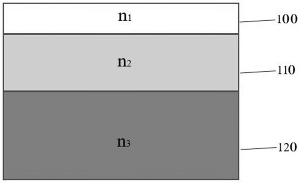
[0028] like figure 1 The on-chip light source modulation system shown is mainly divided into three layers, which are n from bottom to top 3 layer, n 2 layer, n 1 layer, where n 3 layer is a silicon substrate 120, n 2 The layer is a silicon dioxide buried oxide layer 110, n 1 The layer is a silicon nitride layer 100 , the height of the silicon substrate 120 is greater than the height of the silicon dioxide buried oxide layer 110 , and the height of the silicon dioxide buried oxide layer 110 is greater than the height of the silicon nitride layer 100 .

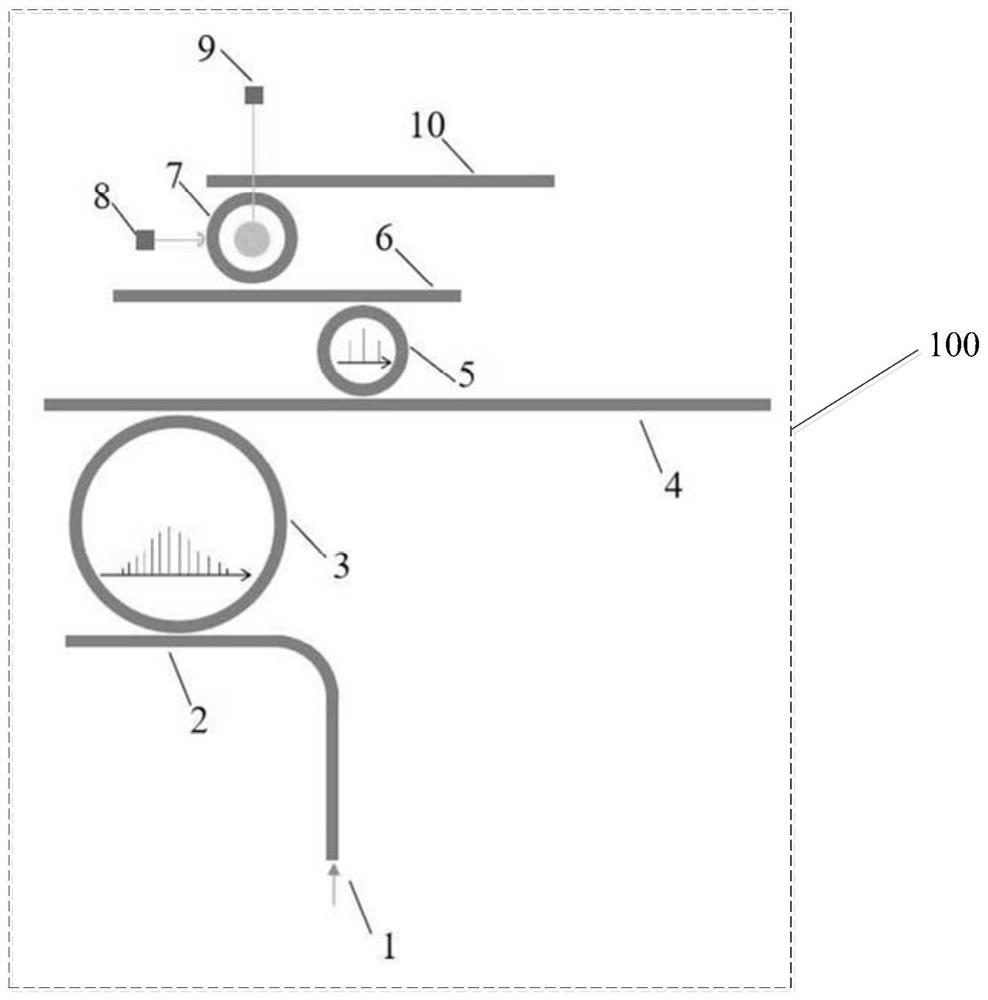
[0029] The structure of the silicon nitride layer 100 is as figure 2 As shown, it mainly includes a microring resonator 3, a microring filter 5, a microring modulator 7 and several waveguides. The radii of the microring modulator 7 and the microring filter 5 are equal, and the radius of the microring resonator 3 is larger than The radius of the microring filter 5. The specific positional relationship between the componen...

Embodiment 2

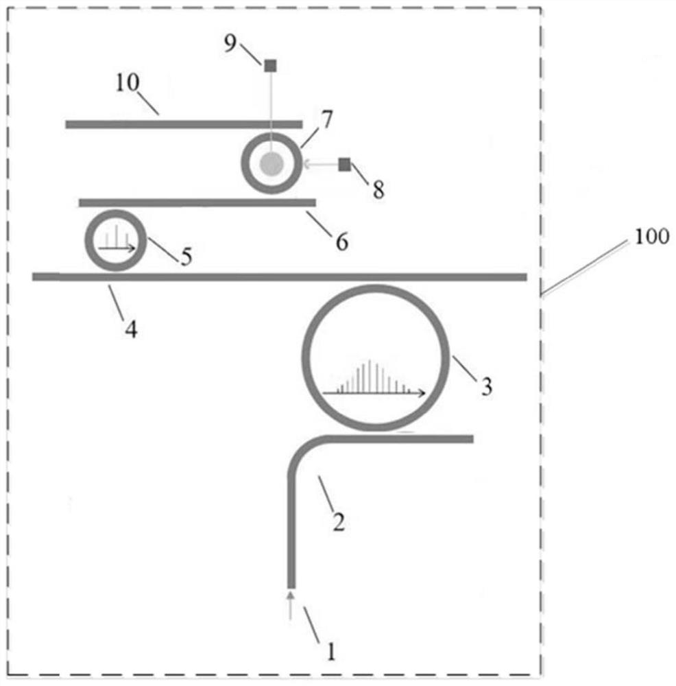
[0051] This embodiment proposes an on-chip light source modulation system, such as image 3 As shown, the system is the same as in Example 1 figure 2 The light source modulation system shown differs in that, figure 2 The micro-ring resonant cavity 3 is located on the left side of the second silicon nitride waveguide 4, the resonant filter 5 is located on the right side of the second silicon nitride waveguide 4 and the third silicon nitride waveguide 6, and the resonant modulator 7 is located on the silicon nitride The left side of the silicon third waveguide 6 and the silicon nitride fourth waveguide 10 .

[0052] In this embodiment, the microring resonant cavity 3 is located on the right side of the second silicon nitride waveguide 4, the resonant filter 5 is located on the left side of the second silicon nitride waveguide 4 and the third silicon nitride waveguide 6, and the resonant modulator 7 is located on the right side of the third silicon nitride waveguide 6 and the...


PUM

PropertyMeasurementUnit
Heightaaaaaaaaaa
Heightaaaaaaaaaa
Heightaaaaaaaaaa

Abstract

The invention discloses an on-chip light source modulation system which comprises a silicon substrate, a silicon dioxide buried oxide layer and a silicon nitride layer, the silicon nitride layer comprises a first waveguide, a second waveguide, a third waveguide and a fourth waveguide which are sequentially arranged, a micro-ring resonant cavity is arranged between the first waveguide and the second waveguide, the distance between the micro-ring resonant cavity and the first waveguide is a first set distance, the distance between the micro-ring resonant cavity and the second waveguide is a second set distance; a micro-ring filter is arranged between the second waveguide and the third waveguide, the distance between the micro-ring filter and the second waveguide is a third set distance, and the distance between the micro-ring filter and the third waveguide is a fourth set distance; a micro-ring modulator is arranged between the third waveguide and the fourth waveguide, the distance between the micro-ring modulator and the third waveguide is a fifth set distance, and the distance between the micro-ring modulator and the fourth waveguide is a sixth set distance. According to the system, the three silicon nitride micro-ring structures are used for processing an input light source, and an optical frequency comb with a wider free spectral range can be generated.

Description

technical field [0001] The invention relates to the technical field of microwave photonics, in particular to an on-chip light source modulation system. Background technique [0002] In the prior art, a mode-locked laser is usually used to obtain an optical frequency comb. For example, the Chinese invention patent application with the publication number CN108923250A proposes an on-chip integrated Fourier mode-locked laser, which includes a semiconductor optical amplifier, a microwave photonic microring Filters, beam splitters, optical isolators and on-chip integrated optical delay lines together form an optical loop to generate optical resonance, thereby obtaining an optical frequency comb. [0003] The advantage of obtaining an optical frequency comb through a mode-locked laser is that it can be integrated on a single chip. The disadvantage is that the spectral width of the optical frequency comb is relatively narrow, and the spectral width can reach more than ten nm, and th...

Claims


Application Information

Patent Timeline
IPC IPC(8): G02F1/35G02F1/01
CPCG02F1/354G02F1/353G02F1/3503G02F1/0102G02F1/0121G02F2203/56
Inventor 闫培光商镇远陈浩张子鸣杨俊波
Owner SHENZHEN UNIV
Why Eureka
Try Eureka