
High-power and high-efficiency on-chip silicon-based dual-mode terahertz signal source structure

A terahertz, high-efficiency technology, applied in the field of terahertz equipment, can solve the problems of low output power, low DC-RF conversion efficiency, and low output power of terahertz sources, so as to increase output power, reduce noise coupling, and achieve good The effect of linearity

Active Publication Date: 2021-12-24
HANGZHOU DIANZI UNIV
View PDF6 Cites 5 Cited by
  • Summary
  • Abstract
  • Description
  • Claims
  • Application Information

AI Technical Summary

Problems solved by technology

[0003] The current silicon-based passive devices have large losses in the terahertz frequency band; while the intrinsic gain of active devices in the terahertz frequency band is low, which will lead to low output power and low DC-RF conversion efficiency of the terahertz source on the silicon substrate
Therefore, in the current research and development process of terahertz sources on silicon substrates, it is extremely important to solve the problems of low output power and low DC-RF conversion efficiency.

Method used


Image

  • High-power and high-efficiency on-chip silicon-based dual-mode terahertz signal source structure
  • High-power and high-efficiency on-chip silicon-based dual-mode terahertz signal source structure
  • High-power and high-efficiency on-chip silicon-based dual-mode terahertz signal source structure

Examples


Embodiment 1

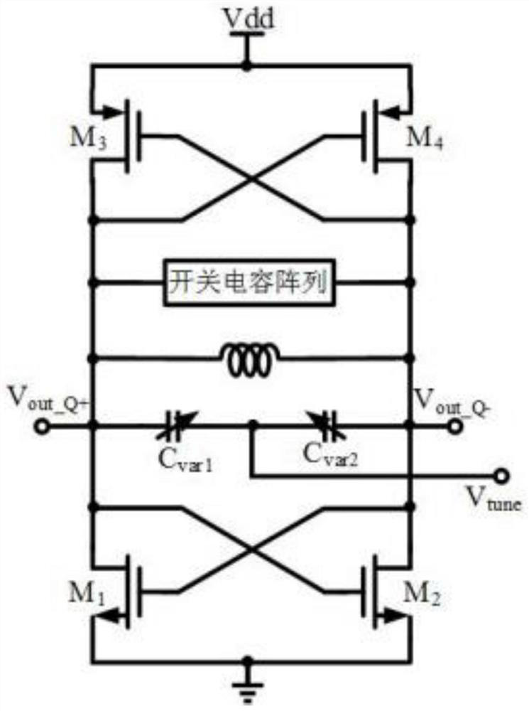
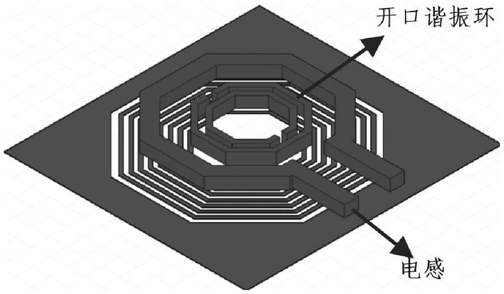
[0032] Such as figure 1 As shown, a high-power, high-efficiency on-chip silicon-based dual-mode terahertz signal source structure includes a driver amplifier, an on-chip power divider, a voltage-controlled oscillator array, a frequency multiplier, and an on-chip combiner. The frequency multiplication link is connected to the on-chip power divider through a switch; the switch is also connected to the voltage-controlled oscillator, and the switch can switch between the voltage-controlled oscillator and the frequency multiplication link; The oscillator array is connected; the voltage-controlled oscillator array includes at least two voltage-controlled oscillators, and the voltage-controlled oscillators in the voltage-controlled oscillator array are arranged in parallel with each other; each voltage-controlled oscillator in the voltage-controlled oscillator array is passed through a multiplier The frequency converter is connected to the on-chip combiner.

[0033] The switching sw...


PUM


Abstract

According to the high-power and high-efficiency on-chip silicon-based dual-mode terahertz signal source structure, output signals in a voltage-controlled oscillator array are set to pass through an on-chip combiner, power output by multiple paths of voltage-controlled oscillators is synthesized, meanwhile, the output power of an active circuit including the voltage-controlled oscillator array and a frequency multiplier circuit is improved, the output power of the terahertz source is improved; the efficiency of the terahertz source is improved by improving the quality factor of the inductor in the voltage-controlled oscillator and reducing the loss of the on-chip combiner; the band-stop network is arranged in the frequency multiplier circuit to be grounded, so that frequency signals are prevented from being leaked to the ground, the signals are output from the output end as far as possible, and power and efficiency are improved.

Description

technical field [0001] The invention relates to the field of terahertz equipment, in particular to an on-chip silicon-based dual-mode terahertz signal source structure with high power and high efficiency. Background technique [0002] Terahertz (TeraHertz, THz) waves refer to electromagnetic waves with a frequency in the range of 0.3-10THz, which is a spectral window of the electromagnetic spectrum between microwaves and far-infrared light. Integrated circuits on silicon substrates based on this frequency band are currently Research hotspots. Among them, terahertz wave has the characteristics of broadband, transient, coherence and penetrability, so it is widely used in communication, medical imaging, radar, remote sensing and other fields. [0003] The current silicon-based passive devices have large losses in the terahertz frequency band; while the intrinsic gain of active devices in the terahertz frequency band is low, which will lead to low output power and low DC-RF con...

Claims


Application Information

Patent Timeline
Patent Type & Authority Applications(China)
IPC IPC(8): H03B5/12H03B19/14H03L7/16
CPCH03B5/1228H03B19/14H03L7/16
Inventor 苏国东王禁城董洪成刘军
Owner HANGZHOU DIANZI UNIV
Learn More