Ultra-wideband low-noise amplification circuit

A low-noise amplification and ultra-broadband technology, which is applied in low-noise amplifiers, amplifiers, radio frequency amplifiers, etc., can solve the problems of low-noise implementation of amplifiers, unsatisfactory gain fluctuations, and insufficient gain, and achieve suppression of circuit instability. The effect of flat gain and high gain

Pending Publication Date: 2022-01-07
CHENGDU GANIDE TECH
View PDF0 Cites 9 Cited by
  • Summary
  • Abstract
  • Description
  • Claims
  • Application Information

AI Technical Summary

Problems solved by technology

[0004] In view of the above-mentioned deficiencies in the prior art, the ultra-wideband low-noise amplifying circuit provided by the present invention solves the problems of difficulty in realizing low noise of the amplifier in multi-octave bands, insufficient gain, unsatisfactory gain fluctuation, and easy instability of the circuit. Provides an amplifying circuit that takes into account low noise and high output power and efficiency within an ultra-wideband

Method used


Image

  • Ultra-wideband low-noise amplification circuit
  • Ultra-wideband low-noise amplification circuit
  • Ultra-wideband low-noise amplification circuit

Examples


Embodiment 1

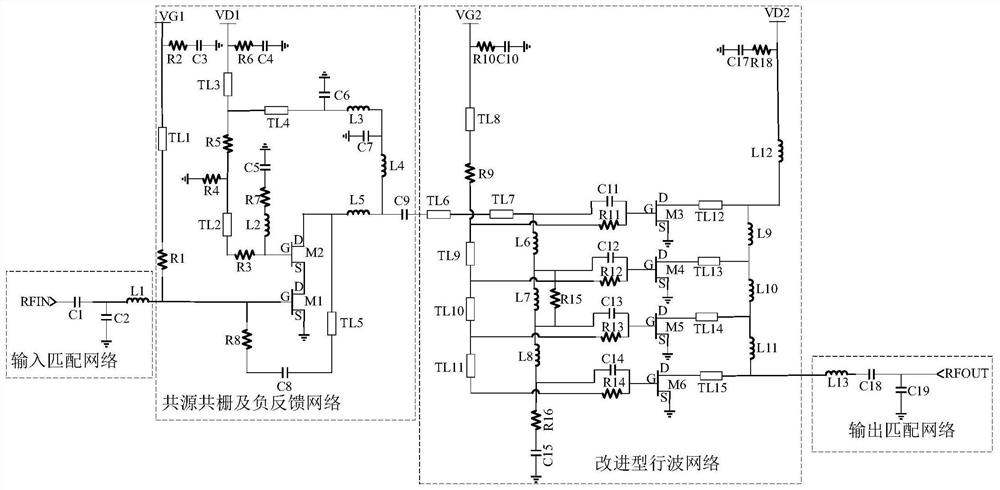
[0036] like figure 1 As shown, an ultra-wideband low noise amplification circuit includes an input matching network, a common source, a negative feedback network, an improved line wave network, and an output matching network;

[0037] Improved traveling wave networks include four transistors, and the gate of each transistor is connected to a microstrip line through a resistor, and the output end of each transistor is connected to an inductance connection;

[0038] Enter the input of the matching network as the input of the ultra-wideband low noise amplification circuit, outputs the output of the matching network as the output of the ultra-wideband low noise amplifier circuit.

[0039] In the present embodiment, the four-channel transistor is the same, and each transistor gate radio frequency input and DC feed are completely separated. The radio frequency passage before the transistor gate is added to a capacitor, and the DC passage is connected by a circuit. The line returns the gat...

Embodiment 2

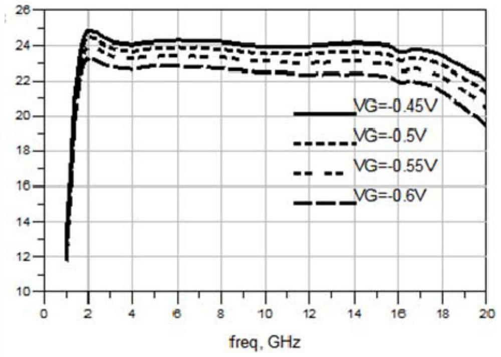
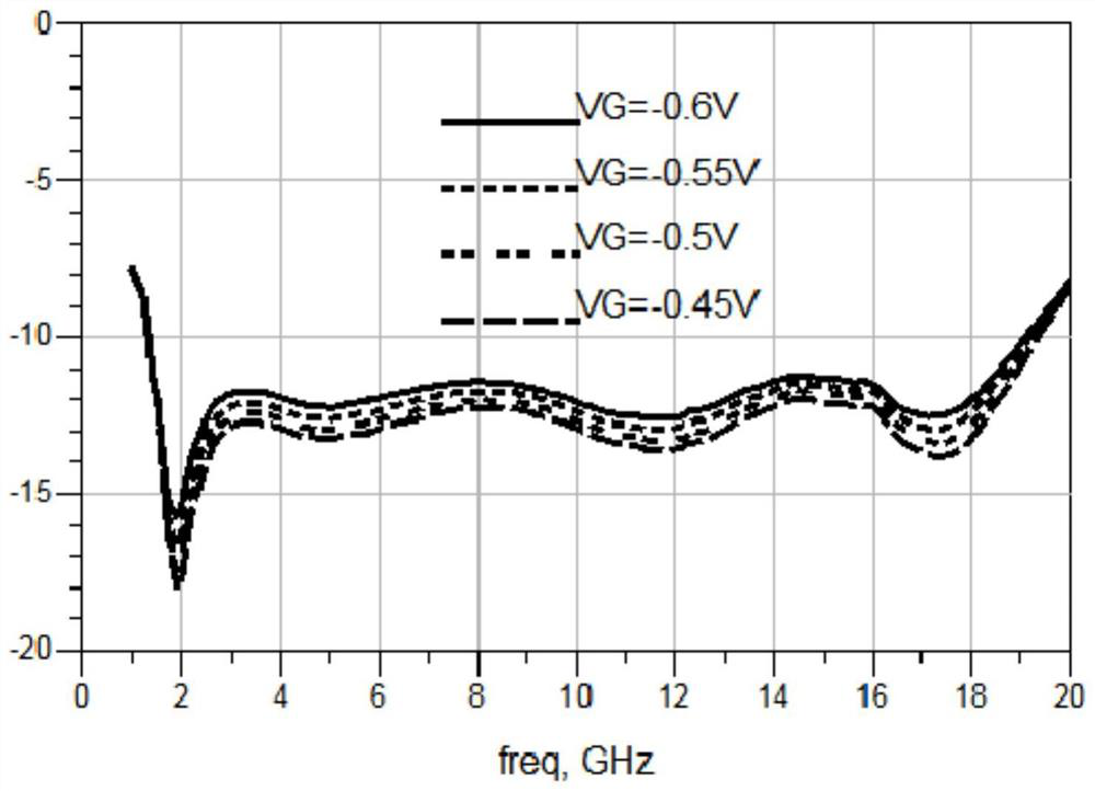
[0053] like Figure 2 ~ 6 As shown, in this embodiment, the above-described amplifying circuit is provided in the frequency band of 2 to 18 GHz, and an echo loss, noise, and output power test curve example;

[0054] Among them, Vd1 = Vd2 = 4V, gate pressure Vg variable, VG1 = Vg2 = -0.45V ~ -0.6V, step = 0.05V, and all-bands no misseb, from the figure, it can be seen that the amplifier is working in Ultra-wide band 2 ~ 18GHz, full range input echo loss is less than -13, output returning loss is less than -15; its gain has typical value 24dB when VG = -0.45, and has gain variable characteristics; full frequency band gain fluctuations less than ± 1dB, and at 4 ~ 16GHz less than ± 0.2dB; the noise is typically 1.5dB; the output P1 is typically 17.5 dBm.


PUM


Abstract

The ultra-wideband low-noise amplification circuit comprises an input matching network, a cascode and negative feedback network, an improved traveling wave network and an output matching network which are connected in sequence. The improved traveling wave network comprises four transistors, the grid voltage end of each transistor is connected with a microstrip line through a resistor, and the output end of each transistor is connected with an inductor through a microstrip line. According to the amplifying circuit, the grid voltage is controllable, a cascode structure, a negative feedback structure and an improved traveling wave network are combined, the bandwidth of the amplifying circuit can be greatly expanded, and better standing waves and flatter gains are achieved in the full frequency band. Besides, the improved traveling wave network is cascaded at the last stage, so that higher gain of the circuit is guaranteed, higher output power and higher efficiency of the circuit can be well realized, and instability of the circuit can be effectively suppressed.

Description

Technical field [0001] The present invention belongs to the field of amplifying circuit design, and more particularly to an ultra-wideband low noise amplifying circuit. Background technique [0002] The modern communication system has increased with the requirements of bandwidth and information capacity, and the emergence of ultra-wideband wireless communication technology can solve the above problems. The low noise amplifier circuit serves as a prodrugate circuit of the ultra-wideband receiver, and its performance is related to key indicators such as overall bandwidth, noise coefficient, sensitivity, linearity. However, an amplifier that wants to design a flat gain, ultra-low noise and a certain output power and efficiency is a challenging work in multiple times. At present, the ultra-wideband low noise amplifier ensures low noise, it is difficult to take into account larger power output; more importantly, the amplifier wants to achieve high gain in the ultra-wide frequency band...

Claims


Application Information

Patent Timeline
IPC IPC(8): H03F1/26H03F1/42H03F1/56
CPCH03F1/26H03F1/42H03F1/56H03F2200/372H03F2200/294H03F2200/36H03F2200/451
Inventor 叶珍刘莹王测天廖学介滑育楠邬海峰吕继平童伟
Owner CHENGDU GANIDE TECH
Why Eureka
Try Eureka