Laminated liquid crystal antenna and manufacturing method thereof
A manufacturing method and liquid crystal technology, applied in nonlinear optics, instruments, optics, etc., can solve the problem of increasing transmission loss, and achieve the effect of reducing transmission loss, enriching functions, and increasing the amount of phase shift
- Summary
- Abstract
- Description
- Claims
- Application Information
AI Technical Summary
Problems solved by technology
Method used
Image
Examples
Embodiment 1
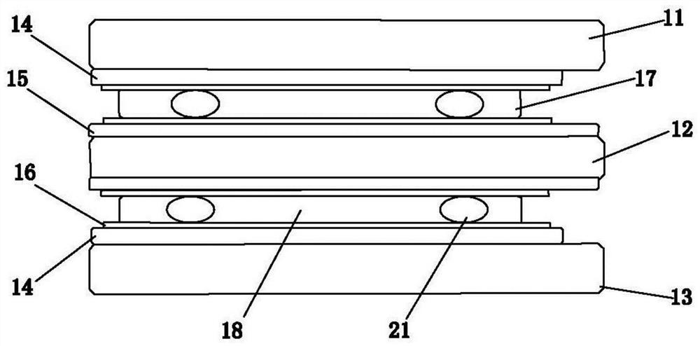
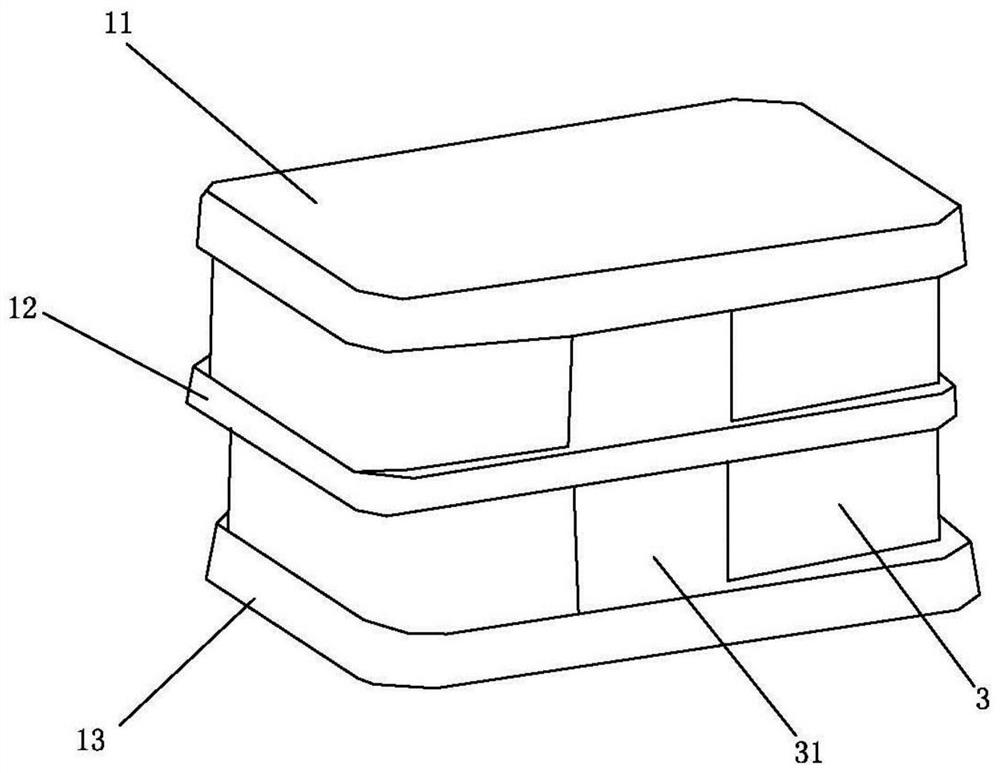
[0042] like figure 1 As shown in a liquid crystal laminate antenna includes an upper electrode substrate 11, the intermediate electrode substrate 12 and the lower electrode substrate 13, the upper electrode substrate 11, the intermediate electrode substrate 12 and the lower electrode substrate 13 is provided the use of superimposed sequentially, three electrode substrate materials include but not limited to plate glass material, a quartz material plate, ceramic plate, a silicon wafer, and the PCB material sheet other polymeric materials such as PET, PI, LCP plate, the electrode substrate may also be employed in some of the leading edge of a flexible product substrate, such as PET, PMMA, PI, and the flexible web material glass substrate, in this document to use glass material as an example.
[0043] In the choice of the thickness of the upper electrode substrate 11, the substrate thickness of the intermediate electrode 12 and the lower electrode substrate 13 are between 0.1-2.0 mm,...
Embodiment 2
[0074] According to the second embodiment differs from that of Embodiment 1 only: The image 3 , Figure 5 , The thickness of the spacer comprises PS (PostSpacer, post spacer) 22 and a column filled with the liquid crystal and a liquid crystal dropwise addition packaged using laminated (ODF) technique.
[0075] When using a liquid crystal dropping lamination (ODF) liquid crystal filling and packaging technology, the need to first upper electrode substrate 11, the lower substrate 13 to complete the front electrode pattern producing PS post 22, the upper electrode film 13 and the lower electrode substrate 11 in the substrate a front coating layer where the thickness of the positive photoresist 2um, at a temperature of 105 ℃ soft bake for 5 minutes. After cooling into the lithography exposure, exposure time 8 seconds, then put in a developing step for developing, water washing after the completion of drying, 150 deg.] C and then hardened for 10 minutes to obtain a highly 8um PS post 22...
PUM
| Property | Measurement | Unit |
|---|---|---|
| thickness | aaaaa | aaaaa |
| thickness | aaaaa | aaaaa |
| thickness | aaaaa | aaaaa |
Abstract
Description
Claims
Application Information


