
Si-based double-sided double-junction AlGaAs solar cell and preparation method thereof

A solar cell, double-sided technology, applied in the field of solar photovoltaic, can solve the problems of high cost, complicated preparation process, unsuitable for large-scale industrial production, etc., to reduce the preparation cost, the preparation process is simple, and it is beneficial to the popularization and popularization of large-scale industrialization Effect

Pending Publication Date: 2022-01-11
BEIJING UNIV OF TECH
View PDF0 Cites 0 Cited by
  • Summary
  • Abstract
  • Description
  • Claims
  • Application Information

AI Technical Summary

Problems solved by technology

However, the existing solar cell preparation technologies are mainly through metal-organic chemical vapor deposition (MOCVD) and molecular beam epitaxy (MBE); the preparation process is complicated and the cost is high, which is not suitable for mass industrial production.

Method used


Image

  • Si-based double-sided double-junction AlGaAs solar cell and preparation method thereof
  • Si-based double-sided double-junction AlGaAs solar cell and preparation method thereof
  • Si-based double-sided double-junction AlGaAs solar cell and preparation method thereof

Examples


Embodiment 1

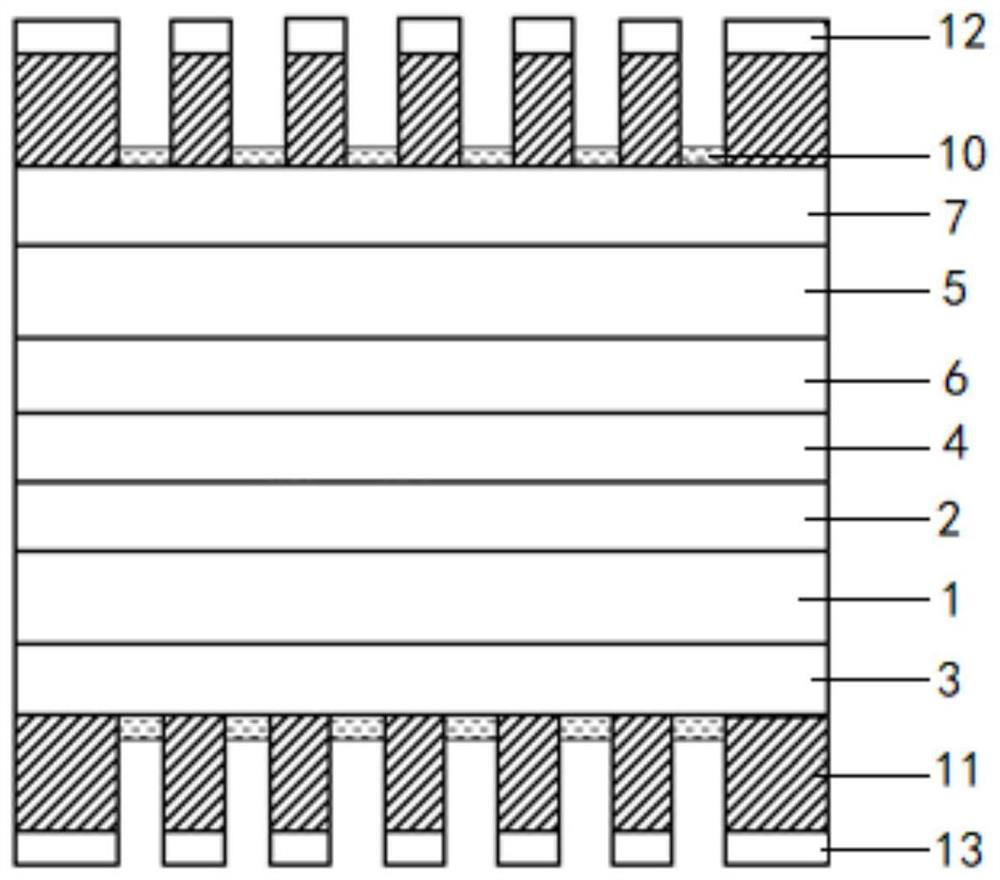
[0056] Such as figure 1 As shown, the present invention provides a Si-based double-sided double-junction AlGaAs solar cell, comprising: an N-type Si substrate 1 and an N-type AlGaAs functional layer 5;

[0057] The N-type Si substrate 1 is double-sided polished, and its upper and lower surfaces are doped to form P + - Si layer 2 and N + -Si layer 3; the upper and lower surfaces of the N-type AlGaAs functional layer 5 are respectively doped to form N + - AlGaAs layer 6 and P + - AlGaAs layer 7, N + -AlGaAs tunnel junction 4 is formed on the AlGaAs layer 6, and the AlGaAs tunnel junction 4 is bonded to the P + - on Si layer 2; P + -An anti-reflection film 10, an ohmic contact layer 11 and a front electrode 12 are formed on the AlGaAs layer 7, N + -An anti-reflection film 10 , an ohmic contact layer 11 and a rear electrode 13 are formed on the Si layer 3 .

[0058] Among them, the N-type AlGaAs functional layer 5, N + - AlGaAs layer 6, P + -AlGaAs layer 7 and AlGaAs tunn...

Embodiment 2

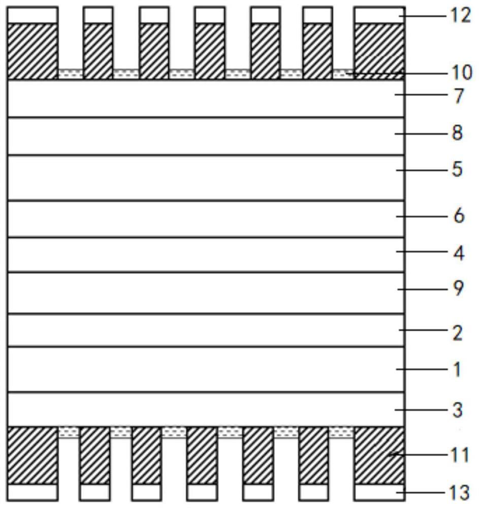
[0066] Such as figure 2 As shown, the present invention provides a Si-based double-sided double-junction AlGaAs solar cell, comprising: an N-type Si substrate 1, an N-type AlGaAs functional layer 5 and a P-type AlGaAs functional layer 8;

[0067] The N-type Si substrate 1 is double-sided polished, and its upper and lower surfaces are doped to form P + - Si layer 2 and N + - Si layer 3; P + -GaAs buffer layer 9, AlGaAs tunnel junction 4, N + -AlGaAs layer 6, N-type AlGaAs functional layer 5, P-type AlGaAs functional layer 8, P + - AlGaAs layer 7; P + -An anti-reflection film 10, an ohmic contact layer 11 and a front electrode 12 are formed on the AlGaAs layer 7, N + -An anti-reflection film 10 , an ohmic contact layer 11 and a rear electrode 13 are formed on the Si layer 3 .

[0068] Among them, the N-type AlGaAs functional layer 5, N + -AlGaAs layer 6 and AlGaAs tunnel junction 4 are Al 0.20 Ga 0.80 As,P + -AlGaAs layer 7 and P-type AlGaAs functional layer 8 are Al ...

Embodiment 3

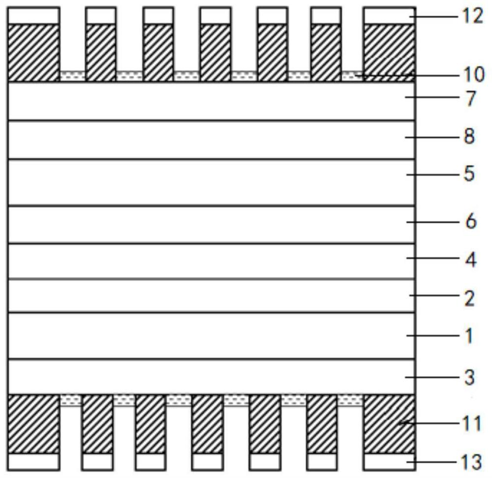
[0079] Such as image 3 As shown, the present invention provides a Si-based double-sided double-junction AlGaAs solar cell, comprising: an N-type Si substrate 1, an N-type AlGaAs functional layer 5 and a P-type AlGaAs functional layer 8;

[0080] The N-type Si substrate 1 is double-sided polished, and its upper and lower surfaces are doped to form P + - Si layer 2 and N + -Si layer 3; the lower surface of the N-type AlGaAs functional layer 5 is doped to form N + - AlGaAs layer 6 and AlGaAs tunnel junction 4, AlGaAs tunnel junction 4 bonded in P + - on the Si layer 2; the P-type AlGaAs functional layer 8 is bonded on the upper surface of the N-type AlGaAs functional layer 5, and the upper surface of the P-type AlGaAs functional layer 8 is doped to form P + - AlGaAs layer 7; P + -An anti-reflection film 10, an ohmic contact layer 11 and a front electrode 12 are formed on the AlGaAs layer 7, N + -An anti-reflection film 10 , an ohmic contact layer 11 and a rear electrode 13 ...


PUM

PropertyMeasurementUnit
Thicknessaaaaaaaaaa
Doping concentrationaaaaaaaaaa
Thicknessaaaaaaaaaa

Abstract

The invention discloses a Si-based double-sided double-junction AlGaAs solar cell and a preparation method thereof. The Si-based double-sided double-junction AlGaAs solar cell comprises an N-type Si substrate and an N-type AlGaAs functional layer; the upper surface and the lower surface of the N-type Si substrate are doped to form a P +-Si layer and an N +-Si layer respectively; the upper surface and the lower surface of the N-type AlGaAs functional layer are doped to form an N +-AlGaAs layer and a P +-AlGaAs layer respectively, an AlGaAs tunnel junction is formed on the N +-AlGaAs layer, and the AlGaAs tunnel junction is bonded on the P +-Si layer; and an antireflection film, an ohmic contact layer and a front electrode are formed on the P < + >-AlGaAs layer, and an antireflection film, an ohmic contact layer and a back electrode are formed on the N < + >-Si layer. According to the invention, the double-sided Si-based solar cell is prepared through wafer bonding and impurity diffusion, so that the preparation cost of the solar cell can be reduced; and in addition, by adopting a wafer bonding mode, the problem of large lattice mismatch between AlGaAs and Si can be effectively solved, and the material performance of the device layer is improved.

Description

technical field [0001] The invention relates to the field of solar photovoltaic technology, in particular to a Si-based double-sided double-junction AlGaAs solar cell and a preparation method. Background technique [0002] Energy, from the industrial revolution to the modern information society, has always been the driving force for the progress and development of social civilization, driving the continuous development of the entire society. From the agricultural society to the industrial society, to today's information age, the development of energy is inseparable. The first energy used by human beings is wood that is easy to obtain on the ground. Further use of coal and oil, etc., the use of a large amount of coal, oil and other fossil fuels has brought a lot of carbon dioxide emissions, causing environmental pollution, greenhouse effect and sea level. A series of problems such as rising. At the same time, the total amount of non-renewable resources such as coal and oil ...

Claims


Application Information

Patent Timeline
IPC IPC(8): H01L31/068H01L31/0687H01L31/18
CPCH01L31/0684H01L31/0687H01L31/18Y02E10/544Y02E10/547Y02P70/50
Inventor 王智勇黄瑞兰天
Owner BEIJING UNIV OF TECH
Learn More