Hafnium oxide-based ferroelectric capacitor and preparation method thereof
A ferroelectric capacitor and hafnium oxide technology, applied in capacitors, circuits, electrical components, etc., can solve the problems of thin film electrical performance degradation, large leakage current of ferroelectric capacitors, and needs to be developed, etc., and achieves mature deposition and etching processes. The effect of resistivity reduction and low power consumption
- Summary
- Abstract
- Description
- Claims
- Application Information
AI Technical Summary
Problems solved by technology
Method used
Image
Examples
preparation example Construction
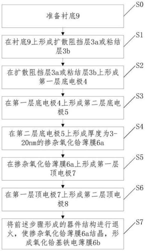
[0069] A preparation method of a hafnium oxide-based ferroelectric capacitor proposed by an embodiment of the present invention, such as figure 2 shown, including the following steps:
[0070] S0, preparing the substrate 9;
[0071] Among them, the substrate 9 is prepared on p-type lightly doped silicon with CMOS addressing, selection and logic control circuits 1, interlayer dielectric 2 is deposited and the planarization process is completed. It can be done in two ways, one is based on the front-end process, that is, the ferroelectric capacitor is embedded before the back-end multi-layer metal wiring process, and after the CMOS addressing, selection and logic control circuits are prepared, the deposition of the first layer of interlayer dielectric is completed And the planarization process, the other is based on the back-end process, that is, the ferroelectric capacitor is embedded in the back-end multi-layer metal wiring process, after the CMOS addressing, selection and lo...
Embodiment 1
[0084] A method for preparing a hafnium oxide-based ferroelectric capacitor provided by an embodiment of the present invention includes the following steps:
[0085] 1) Based on the front-end process, that is, before the ferroelectric capacitor is embedded in the back-end multi-layer metal wiring process, after preparing CMOS addressing, selection and logic control circuits, prepare CMOS addressing, selection and logic control circuits on p-type lightly doped silicon 1. Deposit the interlayer dielectric 2 and complete the planarization process.
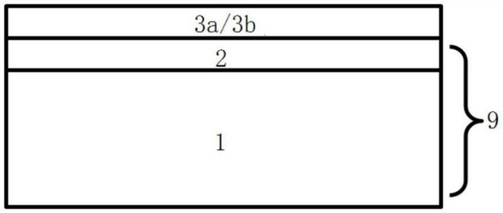
[0086] 2) 10nmTi and 50nmTiN are successively deposited on the substrate 9 by magnetron sputtering method as the diffusion barrier layer 3a or bonding layer 3b (such as figure 1 shown);
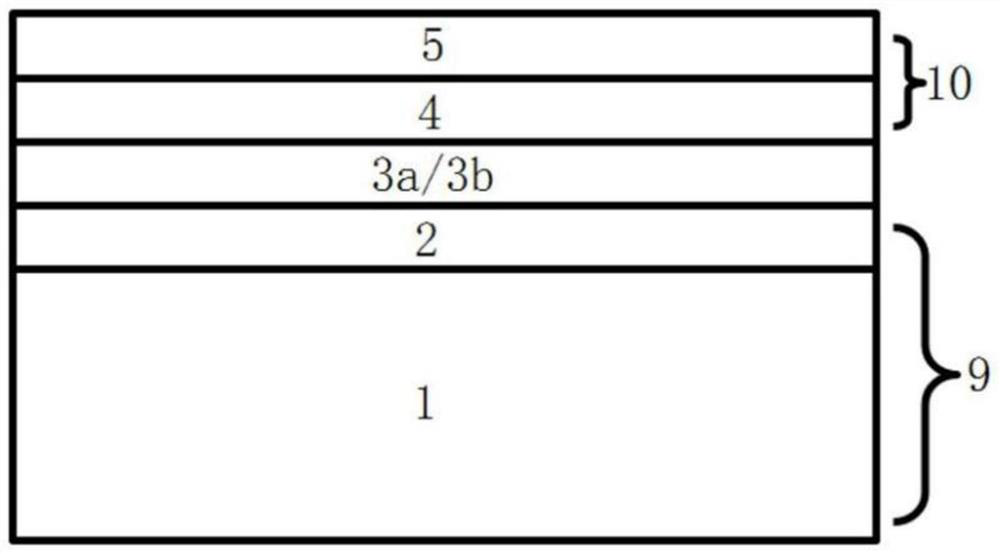
[0087] 3) Deposit the first layer of bottom electrode 4 made of W material on the diffusion barrier layer 3a or the bonding layer 3b by magnetron sputtering method, with a thickness of 50nm, wherein the first layer of bottom electrode 4 is used as a...
Embodiment 2
[0094] A method for preparing a hafnium oxide-based ferroelectric capacitor provided by an embodiment of the present invention includes the following steps:
[0095] 1) Based on the back-end process, that is, after the ferroelectric capacitor is embedded in the back-end multi-layer metal wiring process, after the CMOS addressing, selection and logic control circuits and multi-layer metal wiring process are completed, CMOS is prepared on p-type lightly doped silicon Addressing, selection and logic control circuit 1, deposition of interlayer dielectric 2 and completion of planarization process.
[0096] 2) 10nmTa and 80nmTaN are successively deposited on the substrate 9 by magnetron sputtering as the diffusion barrier layer 3a or bonding layer 3b (such as figure 1 shown);
[0097] 3) Deposit the first layer of bottom electrode 4 made of Cu material on the diffusion barrier layer 3a or the bonding layer 3b by magnetron sputtering method, with a thickness of 100nm, wherein the fi...
PUM
| Property | Measurement | Unit |
|---|---|---|
| thickness | aaaaa | aaaaa |
| thickness | aaaaa | aaaaa |
| thickness | aaaaa | aaaaa |
Abstract
Description
Claims
Application Information


