Semiconductor transistor and preparation method thereof

A technology of transistors and semiconductors, applied in the fields of semiconductor/solid-state device manufacturing, semiconductor devices, electrical components, etc., can solve the problems of electron mobility, lack of high voltage resistance and operating temperature characteristics, low gate voltage resistance, complex process, etc. Achieve the effect of improving product voltage characteristics, increasing breakdown voltage, and strong radiation resistance

Pending Publication Date: 2022-01-18
西安瑞芯光通信息科技有限公司
View PDF0 Cites 0 Cited by
  • Summary
  • Abstract
  • Description
  • Claims
  • Application Information

AI Technical Summary

Problems solved by technology

[0003] At present, silicon-based MOSFETs are very mature in terms of manufacturing process, and silicon-based products also have a huge advantage in terms of price. Compared with third-generation GaN and other materials, silicon’s electron mobility, high-voltage resistance and operating temperature characteristics are lacking. GaN based on the third-generation semiconductor material has been developed such as HEMT (or heterojunction field effect transistor HFET, modulation doped field effect transistor MODFET) devices, and has achieved good results, but there are also problems such as gate withstand voltage Low and complex processes and other issues

Method used


Image

  • Semiconductor transistor and preparation method thereof

Examples


Embodiment 1

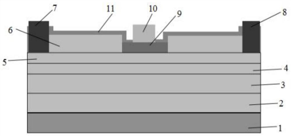
[0039] A semiconductor transistor, comprising an epitaxial layer, an S / D electrode region, a silicon dioxide layer 9, and a G electrode 10;

[0040] Wherein, the S / D electrode region and the silicon dioxide layer 9 are located above the epitaxial layer, and the G electrode 10 is located above the silicon dioxide layer 9;

[0041] The epitaxial layer includes a substrate 1 and a GaN layer 2, a p-GaN layer 3, an i-GaN layer 4, an i-AlN layer 5, and an n-AlGaN layer 6 located above the substrate 1 in sequence;

[0042] The S / D electrode area includes an S electrode 7 and a D electrode 8, and the S electrode 7 and the D electrode 8 are respectively located at both ends of the n-AlGaN layer 6, and the bottom of the n-AlGaN layer 6 is in contact with the top surface of the i-AlGaN layer 5;

[0043] The silicon dioxide layer 9 is located in the middle of the n-AlGaN layer 6, and the bottom penetrates the n-AlGaN layer 6 and contacts the top surface of the i-AlGaN layer 5;

[0044] I...

Embodiment 2

[0055] A semiconductor transistor, comprising an epitaxial layer, an S / D electrode region, a silicon dioxide layer 9, and a G electrode 10;

[0056] Wherein, the S / D electrode region and the silicon dioxide layer 9 are located above the epitaxial layer, and the G electrode 10 is located above the silicon dioxide layer 9;

[0057] The epitaxial layer includes a substrate 1 and a GaN layer 2, a p-GaN layer 3, an i-GaN layer 4, an i-AlN layer 5, and an n-AlGaN layer 6 located above the substrate 1 in sequence;

[0058] The S / D electrode area includes an S electrode 7 and a D electrode 8, and the S electrode 7 and the D electrode 8 are respectively located at both ends of the n-AlGaN layer 6, and the bottom of the n-AlGaN layer 6 is in contact with the top surface of the i-AlGaN layer 5;

[0059] The silicon dioxide layer 9 is located in the middle of the n-AlGaN layer 6, and the bottom penetrates the n-AlGaN layer 6 and contacts the top surface of the i-AlGaN layer 5;

[0060] I...

Embodiment 3

[0071] A semiconductor transistor, comprising an epitaxial layer, an S / D electrode region, a silicon dioxide layer 9, and a G electrode 10;

[0072] Wherein, the S / D electrode region and the silicon dioxide layer 9 are located above the epitaxial layer, and the G electrode 10 is located above the silicon dioxide layer 9;

[0073] The epitaxial layer includes a substrate 1 and a GaN layer 2, a p-GaN layer 3, an i-GaN layer 4, an i-AlN layer 5, and an n-AlGaN layer 6 located above the substrate 1 in sequence;

[0074] The S / D electrode area includes an S electrode 7 and a D electrode 8, and the S electrode 7 and the D electrode 8 are respectively located at both ends of the n-AlGaN layer 6, and the bottom of the n-AlGaN layer 6 is in contact with the top surface of the i-AlGaN layer 5;

[0075] The silicon dioxide layer 9 is located in the middle of the n-AlGaN layer 6, and the bottom penetrates the n-AlGaN layer 6 and contacts the top surface of the i-AlGaN layer 5;

[0076] I...


PUM

PropertyMeasurementUnit
thicknessaaaaaaaaaa
thicknessaaaaaaaaaa
thicknessaaaaaaaaaa

Abstract

The invention discloses a semiconductor transistor and a preparation method thereof. Third-generation semiconductor gallium nitride and a compound thereof are used as epitaxial materials, a P-type region and an N-type region are formed through doping, 2DEG on the surface of a heterojunction material is used as a conductive channel, metal and silicon dioxide are used as a grid electrode, when no voltage is applied to the grid electrode, the source electrode and the drain electrode are equivalent to an N-i-P-i-N structure and cannot be conducted, electrons in N-AlGaN below the source electrode and the drain electrode are attracted to a surface layer by an electric field by applying voltage to the grid electrode, 2DEG formed by AlGaN/GaN at the source electrode and the drain electrode forms a conductive channel, the N-i-P-i-N structure can increase breakdown voltage and improve product voltage characteristics, the conductive channel of the 2DEG can improve the electron mobility, and compared with a multi-sub conductive channel of a semiconductor, the corresponding rate and frequency of a switch are improved.

Description

technical field [0001] The invention relates to the technical field of semiconductor electronic information, and more specifically relates to a semiconductor transistor and a preparation method thereof. Background technique [0002] With the development of semiconductor materials, the design and method of transistors are also constantly improving. At present, the third generation of wide bandgap semiconductors, with their wide bandgap constants, higher electron mobility, strong radiation resistance, and breakdown electric field strength Good, high temperature resistance and other characteristics, has been widely used in the semiconductor field, its chip has the characteristics of high reverse blocking voltage, low forward conduction resistance, high operating frequency, etc., it is an ideal material, especially based on two-dimensional electron gas ( 2DEG) structure, so that the fabricated devices have high electron mobility. [0003] At present, silicon-based MOSFETs are v...

Claims


Application Information

Patent Timeline
Patent Type & Authority Applications(China)
IPC IPC(8): H01L29/06H01L29/778H01L21/335H01L29/49
CPCH01L29/0615H01L29/778H01L29/66462H01L29/495
Inventor 王晓波
Owner 西安瑞芯光通信息科技有限公司
Why Eureka
Try Eureka