
Depletion type power semiconductor structure, series structure and processing technology

A power semiconductor and series structure technology, which is applied in semiconductor devices, semiconductor/solid-state device manufacturing, electrical components, etc., can solve problems such as secondary breakdown, difficult to achieve withstand voltage, and productivity limitations, so as to improve reliability and reduce processing Difficulty, the effect of improving the yield rate

Active Publication Date: 2022-01-21
重庆平创半导体研究院有限责任公司
View PDF8 Cites 2 Cited by
  • Summary
  • Abstract
  • Description
  • Claims
  • Application Information

AI Technical Summary

Problems solved by technology

However, limited by SiO2 / SiC interface defects and productivity, there are currently few units that can produce reliable gate oxide layers for silicon carbide planar MOSFETs, not to mention gate oxide layers for trench MOSFETs with higher current densities and more complex manufacturing processes. layers, so there are still practical manufacturability issues with SiC IGBTs based on MOSFET input stages
[0004]In addition, because in the high-voltage field (6.5kV and above), due to the influence of low doping in the drift region, the parasitic structure of solid-state semiconductor power devices is prone to high-current switching Secondary breakdown occurs. Due to the limitation of secondary breakdown of parasitic structures, it is difficult for solid-state semiconductor power devices to meet the requirements of ultra-high voltage applications such as UHV DC transmission.
Therefore, compared with the use of immature high-voltage single devices, connecting multiple relatively low-voltage devices in series can obtain higher reliability, higher yield, and lower production costs, but the series application is complicated, and the existing technology has no absorption circuit, it is difficult to achieve high-efficiency large-scale series connection

Method used


Image

  • Depletion type power semiconductor structure, series structure and processing technology
  • Depletion type power semiconductor structure, series structure and processing technology
  • Depletion type power semiconductor structure, series structure and processing technology

Examples


Embodiment 1

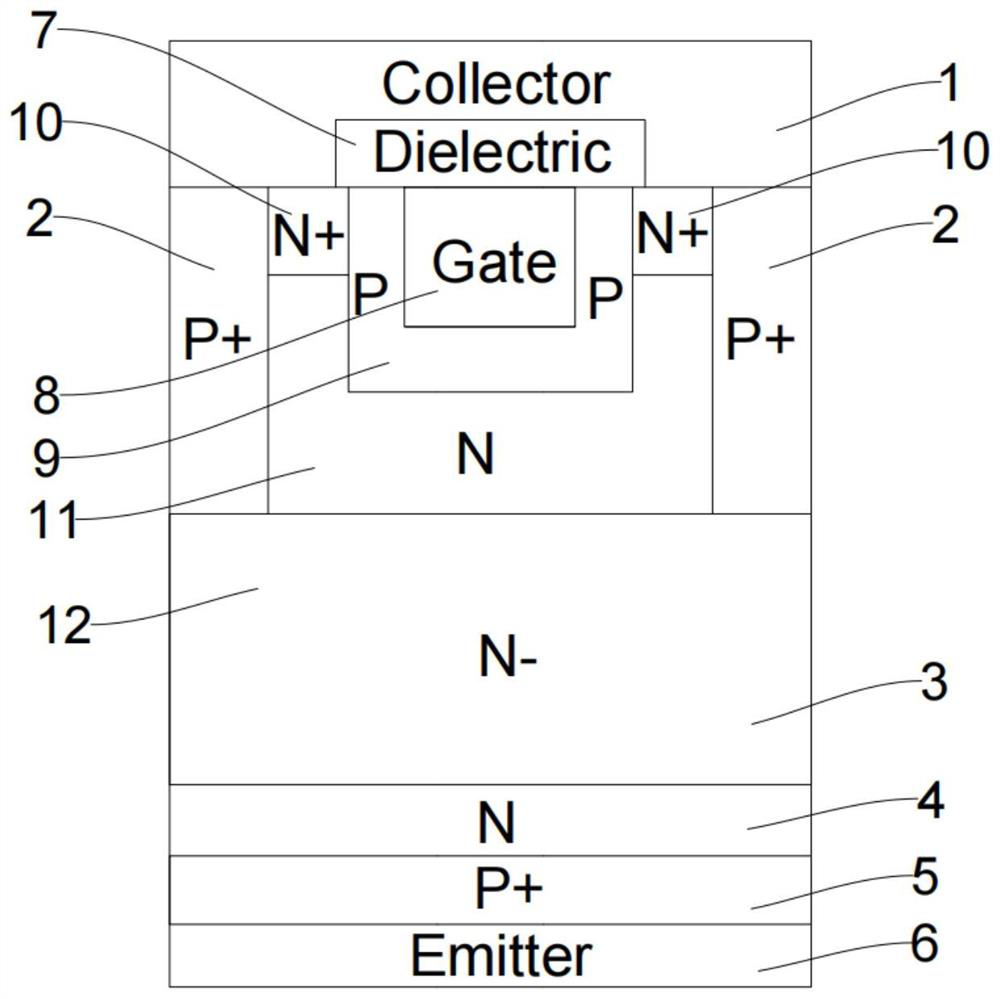
[0070] This embodiment is basically as attached figure 1 Shown: a depletion-type power semiconductor structure, the structure is a semiconductor device, the device is composed of cells arranged in parallel, and its cell structure includes: BJT rear-stage structure and JFET front-stage structure;

[0071] The JFET front-stage structure is set in the BJT post-stage structure, that is, the JFET front-stage structure is used to replace the MOSFET structure of the input stage of the IGBT device. Compared with the MOSFET structure in the IGBT device in the prior art, the gate oxide layer for the silicon carbide planar MOSFET or the gate oxide layer for the trench MOSFET is required, and the JFET front-end structure replaces the MOSFET structure of the input stage of the IGBT device without affecting the original IGBT device. function, and after replacing the MOSFET structure, the JFET front-end structure does not need to set the gate oxide layer for the silicon carbide planar MOSFET...

Embodiment 2

[0086] This embodiment is basically as attached figure 2 Shown: a kind of depletion mode power semiconductor series structure, comprises the depletion mode power device ( figure 2 Medium J1, J2, J3, J4, J5, and J6) and low voltage MOSFETs ( figure 2 M1) in series, the emitter of each depletion power device is connected to the collector of the next depletion power device, and the final depletion power device ( figure 2 The emitter of J6) is connected to the drain of the low-voltage MOSFET, figure 2 Among them, DRAIN represents the positive electrode of the overall device after series connection, GATE represents the control electrode of the entire device after series connection, and SOURCE represents the negative electrode of the entire device after series connection. In this embodiment, six stages are connected in series.

[0087] The gates of each stage of depletion-mode power devices are connected in series with a first resistor ( figure 2 In RG1, RG2, RG3, RG4, RG5...

Embodiment 3

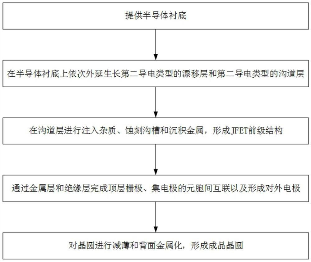
[0092] This embodiment is basically as attached image 3 Shown: a depletion mode power semiconductor structure processing technology, including the following content:

[0093] A semiconductor substrate is provided; the semiconductor substrate includes: a semiconductor substrate of a first conductivity type or a semiconductor substrate of a second conductivity type;

[0094] A drift layer of the second conductivity type and a channel layer of the second conductivity type are epitaxially grown sequentially on the semiconductor substrate; Before the drift layer of the conductivity type and the channel layer of the second conductivity type, a field stop / buffer layer of the second conductivity type is epitaxially grown on the semiconductor substrate;

[0095] Implant impurities, etch trenches and deposit metal in the channel layer to form the JFET front-end structure; specifically:

[0096] Selective implantation of impurities of the first conductivity type and impurities of the ...


PUM


Abstract

The invention relates to the technical field of semiconductor devices, in particular to a depletion type power semiconductor structure, a series structure and a processing technology, and the cellular structure of the depletion type power semiconductor structure comprises a BJT post-stage structure and a JFET pre-stage structure; the JFET pre-stage structure is arranged in the BJT post-stage structure, that is, the JFET pre-stage structure is adopted to replace an MOSFET structure of an IGBT device input stage. The depletion type power semiconductor structure does not need to grow a gate oxide film, so that the practical manufacturability problem caused by arrangement of various gate oxide layers is solved, series connection is easy, and the effects of higher yield and lower production cost can be achieved.

Description

technical field [0001] The invention relates to the technical field of semiconductor devices, in particular to a depletion-type power semiconductor structure, a series structure and a processing technology. Background technique [0002] As solid-state semiconductor power devices gradually penetrate into the application scenarios of traditional gas switches and mechanical switches, the industry has put forward higher requirements for the switching capacity (voltage, current) of solid-state semiconductor power devices. At the same time, the increase in switching frequency plays a key role in reducing the weight of the product. Therefore, the demand for high-voltage, high-current, and high-frequency solid-state semiconductor power devices is imminent. [0003] Among solid-state semiconductor power devices, unipolar devices have good switching performance and are easy to drive. Among them, depletion-type devices have the advantage of being easy to be applied in series; bipolar ...

Claims


Application Information

Patent Timeline
IPC IPC(8): H01L29/739H01L21/331
CPCH01L29/7397H01L29/66348
Inventor 高博陈显平罗厚彩
Owner 重庆平创半导体研究院有限责任公司
Learn More