Processing method of flexible circuit board with thin hollow fingers

A processing method and finger technology, applied in chemical/electrolytic methods to remove conductive materials, printed circuits, printed circuit manufacturing, etc., can solve problems such as wrinkling, distortion, and disconnection of fingers in hollowed out areas, and improve product yield. Effect

Pending Publication Date: 2022-01-21
XIAMEN BOLION CIRCUIT
View PDF0 Cites 2 Cited by
  • Summary
  • Abstract
  • Description
  • Claims
  • Application Information

AI Technical Summary

Problems solved by technology

In the process of product etching and subsequent processing of this kind of flexible circuit board, the fingers in the hollow area are prone to abnormal problems

Method used


Image

  • Processing method of flexible circuit board with thin hollow fingers
  • Processing method of flexible circuit board with thin hollow fingers
  • Processing method of flexible circuit board with thin hollow fingers

Examples


Embodiment Construction

[0027] The present invention will be further described in conjunction with the accompanying drawings and specific embodiments.

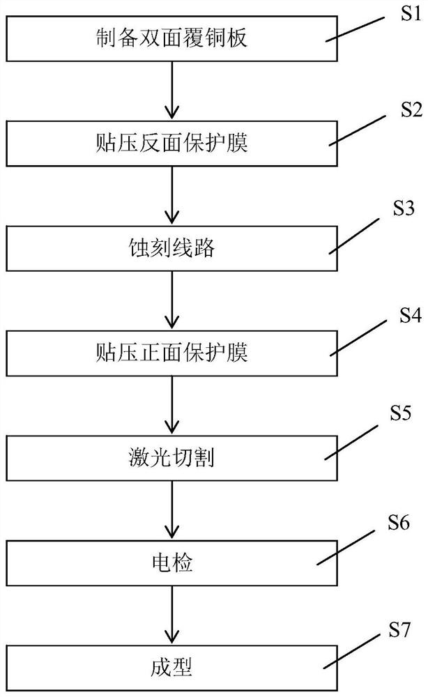
[0028] Such as figure 1 Shown, a kind of processing method of the flexible circuit board that has fine hollow finger (line width less than 0.2 millimeter) can comprise the following steps:

[0029] S1. Prepare a double-sided copper-clad laminate. Specifically, it includes: cutting out double-sided copper-clad laminates of the required shape and size from the raw material FCCL roll; using laser technology to drill pin holes for alignment, direction holes and connections between the two layers of copper layers on the double-sided copper-clad laminates. Via hole. It should be understood that the above-mentioned pin holes, directional holes and via holes may be made by other processing techniques.

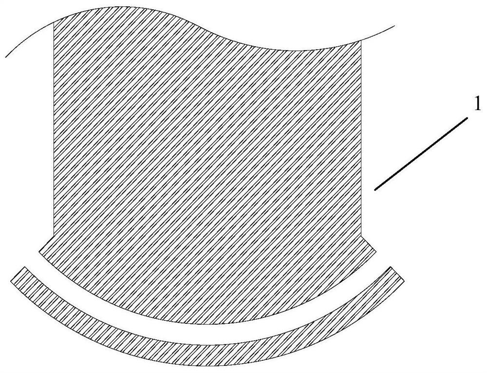
[0030] S2. Paste and press the protective film 1 on the reverse side. First, the reverse protective film 1 is windowed in the hollow area, such as figu...


PUM


Abstract

The invention relates to a processing method of a flexible circuit board with thin hollow fingers. The processing method comprises the following steps: preparing a double-sided copper-clad plate; pasting and pressing a reverse side protection film, windowing the reverse side protection film in the hollow area, and then pasting and pressing the reverse side protection film on the reverse side of the copper-clad plate; etching a circuit, designing thin fingers in the hollow area into a whole, designing a finger extension area exceeding the appearance of the product body, and designing a test disc in the finger extension area; pasting and pressing a front protection film, windowing the front protection film in the hollow area and a test disc, and then pasting and pressing the front protection film on the front surface of the product; carrying out laser cutting, wherein specifically laser cutting is conducted in the hollow area along the edges of the two sides of the fingers, connecting copper between the fingers is cut off, and a hollow finger pattern is completed; carrying out electric detection, wherein an electric detection test needle is placed on the test disc of the finger extension area for electric detection; and forming, wherein specifically, laser or punching forming is adopted, the finger extension area is removed, and final product forming is completed. According to the invention, the hollow finger does not have the problems of wrinkling, deformation and the like in the machining process, and the product yield is greatly improved.

Description

technical field [0001] The invention belongs to the field of flexible circuit boards, and in particular relates to a processing method for a flexible circuit board with thin hollow fingers. Background technique [0002] Flexible Printed Circuit (FPC for short) is a highly reliable and excellent flexible printed circuit board made of polyimide or polyester film, with high wiring density and low weight. Light, thin, and good bendability. [0003] In order to facilitate soldering, some flexible circuit boards have thin hollow fingers (ie, the line width is less than 0.2mm). In the process of product etching and subsequent processing of this kind of flexible circuit board, fingers in the hollow area are prone to abnormal problems such as wrinkling, distortion and even disconnection, which makes production and processing extremely difficult and the yield rate is extremely low. Contents of the invention [0004] The present invention aims to provide a method for processing a f...

Claims


Application Information

Patent Timeline
IPC IPC(8): H05K3/04H05K3/28H05K3/02H05K3/06
CPCH05K3/04H05K3/28H05K3/022H05K3/06
Inventor 王文宝洪诗阅王文峰洪超育
Owner XIAMEN BOLION CIRCUIT
Why Eureka
Try Eureka