Global shutter photosensitive detector based on composite dielectric gate PN junction and working method

A technology of photosensitive detectors and composite media, which is applied to electric solid-state devices, semiconductor devices, components of color TVs, etc., can solve the problems of lack of global shutter structure, decrease of full well charge, and restriction of dynamic object imaging, so as to avoid Effect of dark current noise, space saving, effect of high fill factor

Pending Publication Date: 2022-01-28
NANJING UNIV
View PDF1 Cites 0 Cited by
  • Summary
  • Abstract
  • Description
  • Claims
  • Application Information

AI Technical Summary

Problems solved by technology

If it is used to dope a layer of P-type isolation region around it, it will bring problems such as the decrease of full well charge.
In addition, the detector lacks a global shutter structure inside the device. Currently, imaging can only be read by rolling shutter exposure, which severely restricts the imaging of dynamic objects.

Method used


Image

  • Global shutter photosensitive detector based on composite dielectric gate PN junction and working method
  • Global shutter photosensitive detector based on composite dielectric gate PN junction and working method
  • Global shutter photosensitive detector based on composite dielectric gate PN junction and working method

Examples


Embodiment Construction

[0032] In order to make the object, technical solution and advantages of the present invention clearer, the embodiments of the present invention will be further described in detail below in conjunction with the accompanying drawings.

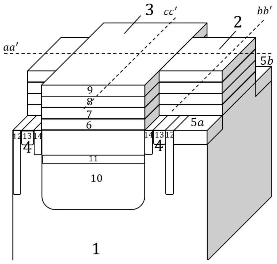
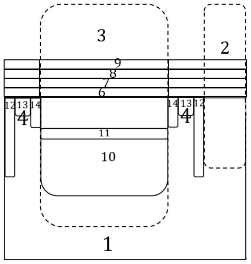
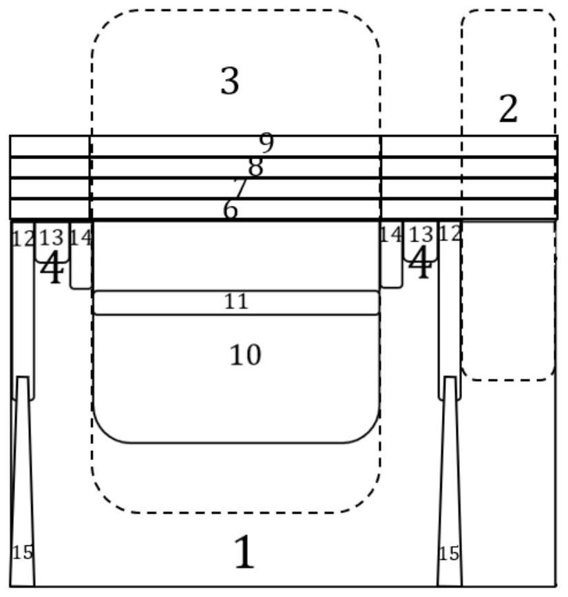
[0033] This embodiment provides a device structure of a global shutter photosensitive detector based on a composite dielectric gate PN junction. The detector unit is fabricated on the same P-type substrate, including a composite dielectric gate transistor 2 with a read function and a photosensitive The composite dielectric gate MOS capacitor 3 is used, and the doped region 4 with the function of realizing the global shutter and the isolation function is arranged in the substrate between the two.

[0034] like figure 1 As shown, the transistor 2 and the MOS capacitor 3 of the detector unit share a composite dielectric gate, which includes a bottom insulating dielectric layer 6, a floating gate 7, a top dielectric layer 8, and a control gate 9 fro...


PUM


Abstract

The invention discloses a global shutter photosensitive detector based on a composite dielectric gate PN junction. The unit comprises a composite dielectric gate MOS capacitor, a composite dielectric gate transistor and global shutter structures which are formed above the same P-type semiconductor substrate, wherein the composite dielectric gate transistor comprises a source drain region, a bottom insulating dielectric layer, a floating gate, a top insulating dielectric layer and a control gate; according to the composite dielectric gate MOS capacitor, a bottom insulating dielectric layer, a floating gate, a top insulating dielectric layer and a control gate are sequentially arranged on a substrate; the global shutter structures are arranged on the two sides of the composite dielectric gate MOS capacitor, each global shutter structure comprises a P or P+ type doped isolation region and an N+ type doped region, and photoelectron collection opening and closing during light sensing of the MOS capacitor are achieved by controlling the voltage on the N+ type doped regions. According to the invention, the global exposure function of the detector can be realized without additionally occupying the space of the detector unit, and the influence of dark current noise at the existing shallow trench isolation interface can be avoided.

Description

technical field [0001] The invention relates to the structure and working mechanism of an imaging detection device, especially an imaging detection device in the infrared, visible light band to ultraviolet band, and specifically relates to a photosensitive detector based on a composite dielectric grid PN junction global shutter structure and its working method. Background technique [0002] The current common CMOS-APS is usually composed of a photodiode and three to six transistors, and more complex functions are realized by means of transistor division. CMOS-APS adopts X-Y addressing mode to read signals, so its imaging speed is faster than CCD. At the same time, CMOS-APS is compatible with CMOS technology and is easy to integrate with peripheral circuits. However, because the pixel contains multiple transistors, the fill factor of the pixel is low, which makes the full well charge of CMOS-APS low. In order to ensure high imaging quality, it is difficult to further reduce t...

Claims


Application Information

Patent Timeline
Patent Type & Authority Applications(China)
IPC IPC(8): H01L27/146H04N5/374
CPCH01L27/14614H01L27/14603H01L27/14643H04N25/76
Inventor 闫锋常峻淞沈凡翔王子豪陈辉李张南王凯胡心怡顾郅扬柴智
Owner NANJING UNIV
Why Eureka
Try Eureka