A CVD-based strained diamond growth doping method

A diamond and diamond layer technology, applied in metal material coating process, coating, gaseous chemical plating and other directions, can solve the problems of difficult doping, high formation energy, limiting the electrical properties of n-type diamond, and reduce the resistivity. Effect

Active Publication Date: 2022-03-15
WUHAN UNIV
View PDF9 Cites 0 Cited by
  • Summary
  • Abstract
  • Description
  • Claims
  • Application Information

AI Technical Summary

Problems solved by technology

In addition, many scholars have proposed n-type co-doped diamond. Although its ionization energy is lower than that of phosphorus, it is still limited by the higher formation energy of the co-doped structure, which makes it difficult to dope in the actual process.
Other single doping elements, such as oxygen, sulfur, and arsenic, have the disadvantage of high formation energy, which limits the electrical properties of n-type diamond

Method used


Image

  • A CVD-based strained diamond growth doping method
  • A CVD-based strained diamond growth doping method
  • A CVD-based strained diamond growth doping method

Examples


Embodiment Construction

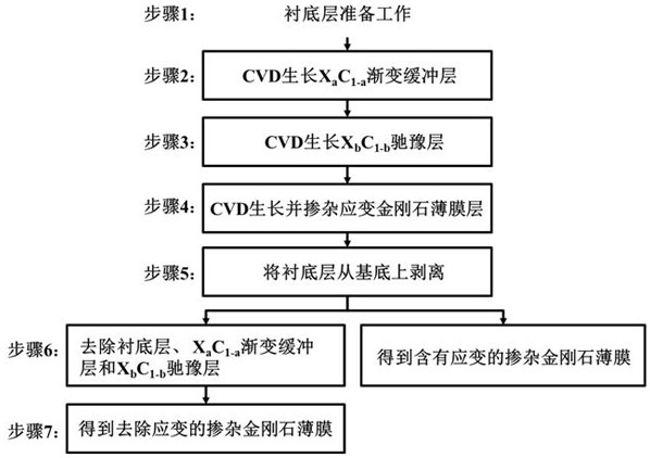
[0021] Below in conjunction with accompanying drawing and specific embodiment the present invention will be described in further detail:

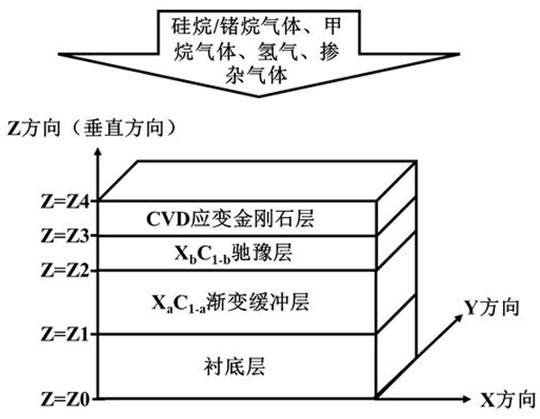
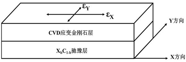
[0022] Such as figure 1 As shown, the present invention provides a strained diamond growth doped epitaxial structure based on the CVD method, through the CVD method, from bottom to top in the vertical direction, sequentially deposit X on the substrate layer a C 1-a Gradient Buffer, X b C 1-b relaxation layer, eventually at X b C 1-b A layer of CVD strained diamond is deposited on top of the relaxed layer.

[0023] Such as figure 1 As shown, the vertical thickness of the substrate layer material is between Z=Z0 and Z=Z1.

[0024] Such as figure 1 Shown, X a C 1-a The vertical thickness of the gradient buffer layer is between Z=Z1 and Z=Z2.

[0025] Such as figure 1 Shown, X b C 1-b The vertical thickness of the relaxed layer is between Z=Z2 and Z=Z3.

[0026] Such as figure 1 As shown, the vertical thickness of the CVD strain...


PUM

PropertyMeasurementUnit
electrical resistivityaaaaaaaaaa
thicknessaaaaaaaaaa
thicknessaaaaaaaaaa

Abstract

The invention relates to a strained diamond growth doping method based on a CVD method. A graded buffer layer and a relaxation layer are sequentially deposited on the substrate layer by a CVD method, and finally a CVD strained diamond layer is deposited on the relaxation layer, and doped by a CVD method. In the method, the lattice constant of the relaxed layer prepared by the CVD method is larger than that of diamond, thereby causing the diamond to generate tensile strain. During the growth and doping process of CVD strained diamond, the diamond is in a state of tensile strain. Therefore, the formation energy of doping elements is low, and it is easy to incorporate into diamond, so that the doping concentration of diamond is higher.

Description

technical field [0001] The invention belongs to the technical field of diamond semiconductors, and relates to a vapor deposition process, in particular to a method for growing and doping strained diamond based on a CVD method. Background technique [0002] Diamond is a colorless and transparent material composed of carbon atoms in a face-centered cubic structure. Carbon and carbon are connected by sp3 covalent bonds. face centered cubic structure and sp 3 Covalent bonds make diamond exhibit high hardness, high thermal stability and high chemical stability. Pure diamond is an insulator with a resistivity as high as 10 13 -10 16 Ω m, at a temperature of 300K, the diamond band gap reaches 5.47eV, and the electron mobility reaches (4500cm 2 ·V −1 ·s −1 ). By doping elements such as nitrogen or boron, diamond can have the properties of n-type semiconductor and p-type semiconductor respectively. As a third-generation semiconductor, diamond is also known as the ultimate se...

Claims


Application Information

Patent Timeline
Patent Type & Authority Patents(China)
IPC IPC(8): C23C16/27C23C16/02
CPCC23C16/278C23C16/0272C30B29/04C30B25/183C30B25/18
Inventor 刘胜沈威吴改郭宇铮梁康汪启军王诗兆
Owner WUHAN UNIV
Why Eureka
Try Eureka