Substrate-free high-power amplitude limiter and preparation method thereof

A substrate-free, high-power technology, which is applied in the fields of diode amplitude limitation, semiconductor/solid-state device manufacturing, and electric solid-state devices, can solve problems such as difficulty in meeting the needs of high-power limiting applications and low thermal conductivity, and achieve improved Withstand power, effect of low series resistance

Pending Publication Date: 2022-02-08
南京中电芯谷高频器件产业技术研究院有限公司
View PDF7 Cites 1 Cited by
  • Summary
  • Abstract
  • Description
  • Claims
  • Application Information

AI Technical Summary

Problems solved by technology

[0004] The purpose of the present invention is to provide a substrate-less high-power limiter and its preparation method, which solves the problem of the low thermal conductivity of the substrate material of Si or GaAs in the existing Si or GaAs PIN limiter diodes. Problems with High Power Limiting Application Requirements

Method used


Image

  • Substrate-free high-power amplitude limiter and preparation method thereof
  • Substrate-free high-power amplitude limiter and preparation method thereof
  • Substrate-free high-power amplitude limiter and preparation method thereof

Examples


preparation example Construction

[0028] A substrate-free high-power limiter and a preparation method thereof, comprising the following steps:

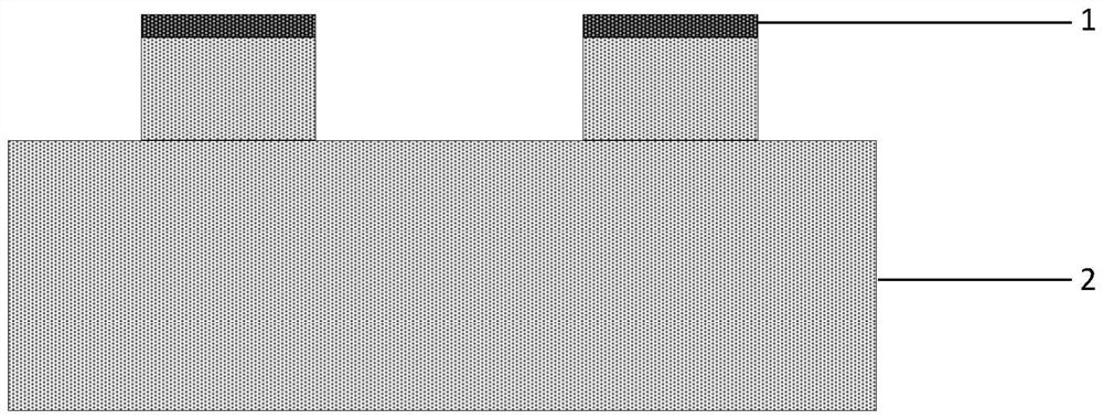
[0029] ① Prepare the PIN limiter tube front process on the surface of the PIN limiter diode 2 material, and etch to expose the P + , I and N + The mesa structure is used to prepare the metal upper electrode 1: wherein the PIN clipping diode material is one of Si and GaAs PIN, and the P + The mesa height of layer I is 0.5-3μm, the height of I-layer mesa is 1μm-20μm, N + The mesa height of the layer is 1-5 μm. The metal upper electrode material includes but not limited to one or a combination of Ti, Pt, Au, Pd, Ni, Al, and the preparation methods include but not limited to evaporation, electroplating, sputtering shoot, etc., such as figure 1 shown.

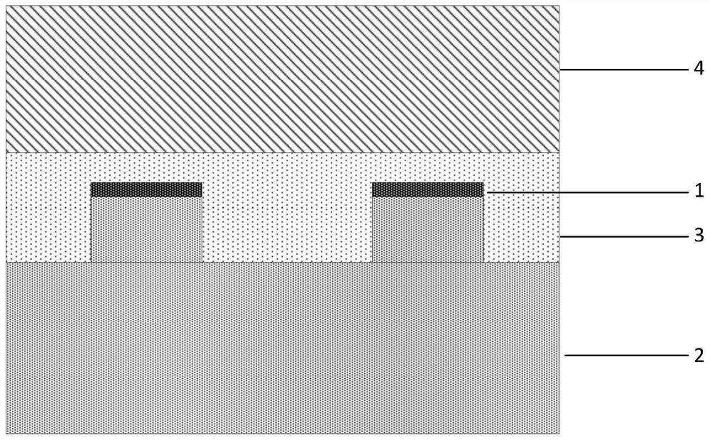
[0030] ② Spin-coat adhesive 3 on the front of the material containing the PIN diode mesa structure: the adhesive 3 is one of polymers such as photoresist, high-temperature wax or BCB, with a thickness of 5-50 μm, and th...

Embodiment

[0036] A substrate-free high-power limiter and a preparation method thereof, comprising the following steps:

[0037] ① Prepare P+, ​​I and N+ mesa structures on Si PIN material wafers, where P + The mesa height of layer I is 1.5 μm, the mesa height of I layer is 8 μm, N + layer mesa height is 3µm, then the P + TiPtAu is evaporated on the layer mesa as the upper electrode metal.

[0038] ② Spin-coat high-temperature wax of about 15 μm on the front surface of the wafer with the PIN mesa structure, the spin-coating speed is 500 rpm, the spin-coating time is 60s, the pre-baking temperature is 155°C, and the time is 5 minutes.

[0039] ③The front side of the wafer containing the PIN mesa structure and the front side of the silicon carrier are relatively bonded together, and put into the chip bonder for temporary bonding. The bonding process parameters are temperature 180°C, bonding time 20 minutes, and bonding pressure 600MPa .

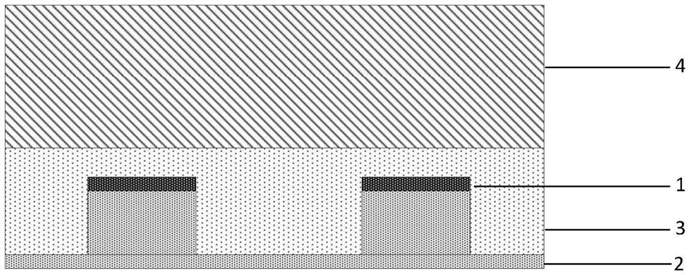
[0040] ④ The Si PIN wafer is ground and thinned...


PUM

PropertyMeasurementUnit
electrical resistivityaaaaaaaaaa
thicknessaaaaaaaaaa
heightaaaaaaaaaa

Abstract

The invention discloses a substrate-free high-power amplitude limiter and a preparation method thereof, and the method comprises the steps: preparing a PIN amplitude limiting tube front surface technology on the surface of a PIN amplitude limiting diode material, carrying out the etching of a mesa structure which exposes P+, I and N+, and preparing a metal upper electrode; performing the spin coating of the front surface of the material containing the PIN diode mesa structure with an adhesive; oppositely and temporarily bonding with the front surface of the temporary slide; thinning and removing the residual substrate; preparing a metal lower electrode on the back surface of the PIN diode material after the substrate is removed; separating the temporary slide glass, and cleaning and scribing the slide glass to obtain the high-power amplitude limiter consisting of a PIN amplitude limiting diode without a substrate and a metal electrode positioned on the back surface of the diode. According to the invention, the Si/GaAs substrate of the traditional PIN amplitude limiting diode is removed, the metal with higher thermal conductivity is used, and meanwhile, the metal material has lower series resistance compared with a semiconductor, so that the tolerance power of the PIN amplitude limiting tube is further improved.

Description

technical field [0001] The invention relates to a substrateless high-power limiter and a preparation method thereof, belonging to the technical field of semiconductors. Background technique [0002] With the application of high-power chips such as GaN, the transmission power of phased array radar is increasing, and it is urgent to increase the withstand power of the limiter in the receiving component to protect the sensitive components of the low-noise amplifier from being affected by external Burned by high-power signals or internal leakage signals. The limiter based on PIN diode is the mainstream application of high-power limiter at present. PIN diode will produce conductance modulation effect under the action of microwave high-power signal, and realize the effect of greatly attenuating the input signal. [0003] In recent years, with the application of high-power radar, in the traditional Si or GaAs PIN limiter, due to the low thermal conductivity of the Si or GaAs subst...

Claims


Application Information

Patent Timeline
Patent Type & Authority Applications(China)
IPC IPC(8): H01L29/868H01L21/329H01L29/417H01L23/373H03G11/02
CPCH01L29/868H01L29/6609H01L29/417H01L23/3736H03G11/02
Inventor 戴家赟孔月婵王飞吴立枢郭怀新陈堂胜
Owner 南京中电芯谷高频器件产业技术研究院有限公司
Why Eureka
Try Eureka