
Memristor based on doped two-dimensional halide perovskite thin film and preparation method of memristor

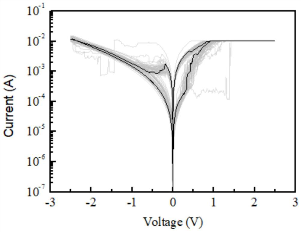
A halide perovskite, memristor technology, applied in electrical components and other directions, to achieve the effect of excellent transport characteristics

Pending Publication Date: 2022-02-08
SHAANXI UNIV OF SCI & TECH
View PDF11 Cites 0 Cited by
  • Summary
  • Abstract
  • Description
  • Claims
  • Application Information

AI Technical Summary

Problems solved by technology

[0005] However, at present, there is no report on the preparation of modified two-dimensional organic-inorganic halide perovskite PEA2PbBr4 by solution method to construct memristors.

Method used


Image

  • Memristor based on doped two-dimensional halide perovskite thin film and preparation method of memristor
  • Memristor based on doped two-dimensional halide perovskite thin film and preparation method of memristor
  • Memristor based on doped two-dimensional halide perovskite thin film and preparation method of memristor

Examples


preparation example Construction

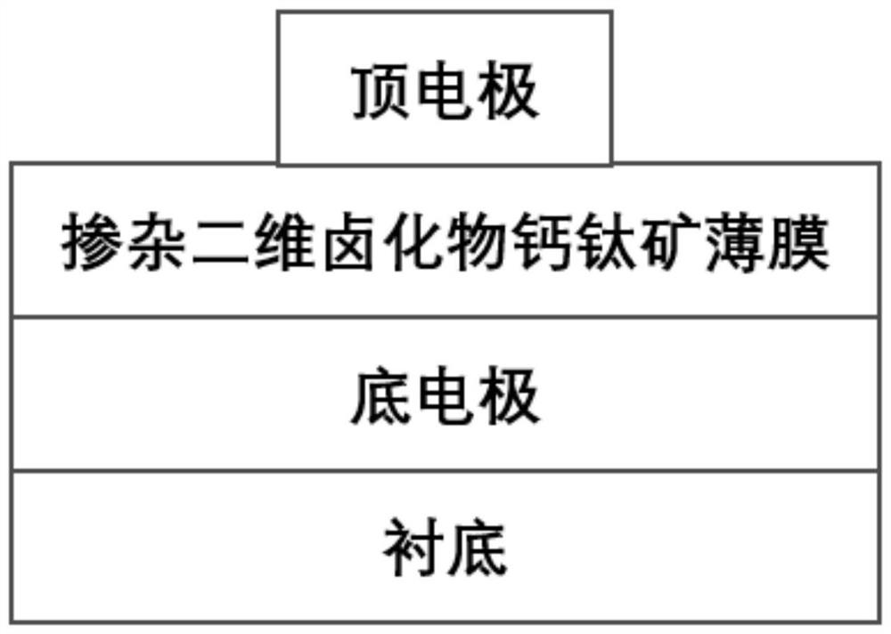
[0048] The present invention is based on a method for preparing a doped two-dimensional halide perovskite thin film memristor, comprising the following steps:

[0049] S1. Select conductive glass or silicon wafer as the substrate, and deposit a conductive film with a thickness of 80 to 200 nanometers on the substrate as the bottom electrode of the device by sputtering or deposition process;

[0050] S2. Mix the nanoparticles and the two-dimensional organic-inorganic halide perovskite according to the mass ratio of (1-50):100, dissolve them in excess dimethyl sulfoxide solution, and ultrasonically treat them in a water bath for 10-60 minutes , to obtain a precursor solution for depositing a resistive switchable thin film; the configured precursor solution is spin-coated on the substrate at a speed of 500-3000rpm, and the spin-coating time is 30-90s. In the last 5-15 seconds of spin-coating, chlorobenzene is added as Anti-solvent; then anneal at 100-200°C for 10-50 minutes in a ...

Embodiment 1

[0060] 1) Select conductive glass as the substrate, and deposit a conductive film with a thickness of 100 nm on the substrate as the bottom electrode of the device by using a sputtering process.

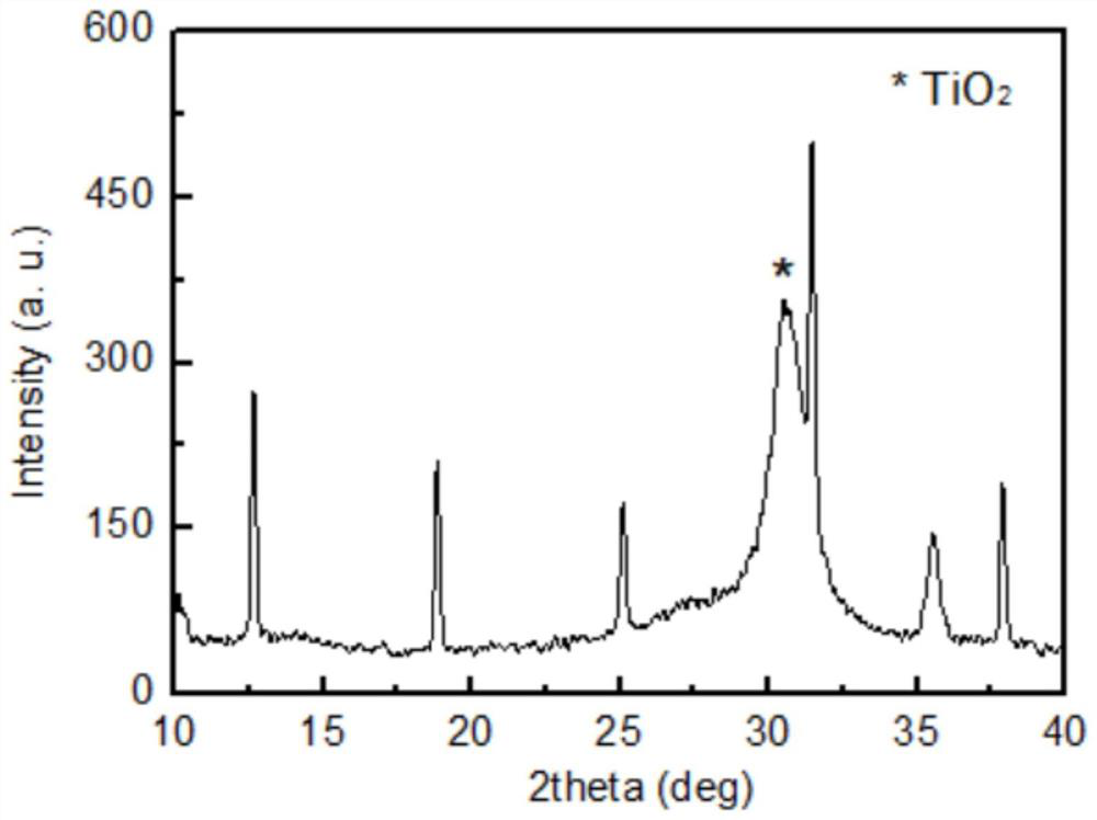
[0061] 2) TiO 2 Nanoparticles and two-dimensional organic-inorganic halide perovskite PEA 2 PbBr 4 Mixed together according to the mass ratio of 3:100, dissolved in excess dimethyl sulfoxide solution, and ultrasonically treated in a water bath for 20 minutes to obtain a precursor solution for depositing a resistive switching film; spin-coat the configured solution at a speed of 3000rpm on On the substrate, the spin-coating time is 60s. In the last 10s of spin-coating, chlorobenzene is added as an anti-solvent; then annealed at 120°C for 20 minutes in a high-purity argon environment, and TiO is obtained after natural cooling. 2 Nanoparticle-doped two-dimensional halide perovskite thin film as a memory layer.

[0062] 3) A circular mask with a diameter of 100 μm is used, and a metal...

Embodiment 2

[0069] 1) Select conductive glass as the substrate, and deposit a conductive film with a thickness of 100 nm on the substrate as the bottom electrode of the device by using a sputtering process.

[0070] 2) TiO 2 Nanoparticles and two-dimensional organic-inorganic halide perovskite PEA 2 PbBr 4 Mix together according to the mass ratio of 50:100, dissolve in excess dimethyl sulfoxide solution, and ultrasonically treat in a water bath for 20 minutes to obtain a precursor solution for depositing a resistive switching film; spin-coat the prepared solution at a speed of 3000rpm on On the substrate, the spin-coating time is 60s. In the last 10s of spin-coating, chlorobenzene is added as an anti-solvent; then annealed at 120°C for 20 minutes in a high-purity argon environment, and TiO is obtained after natural cooling. 2 Nanoparticle-doped two-dimensional halide perovskite thin film as a memory layer.

[0071] 3) Using a circular mask with a diameter of 100 μm, a metal aluminum fi...


PUM

PropertyMeasurementUnit
Diameteraaaaaaaaaa
Thicknessaaaaaaaaaa
Thicknessaaaaaaaaaa

Abstract

The invention discloses a memristor based on a doped two-dimensional halide perovskite thin film and a preparation method of the memristor. The preparation method comprises the steps of selecting a substrate, and depositing a conductive thin film on the substrate to serve as a bottom electrode; doping oxide nano-particles with two-dimensional halide perovskite to form a film on the bottom electrode, wherein the film is used as a storage layer of the resistive device; and depositing a conductive thin film on the resistive random access memory layer as a top electrode. The memristor based on the doped two-dimensional halide perovskite thin film prepared by the method has the advantages of simple structure, high stability, wide material source, low cost and simple preparation process, is beneficial to large-scale application, and has a good market application prospect.

Description

technical field [0001] The invention belongs to the technical field of nonvolatile memory, and in particular relates to a doped two-dimensional halide perovskite thin-film memristor and a preparation method thereof. Background technique [0002] Memristor, due to its simple structure, high storage density, fast read and write speed, low power consumption and easy integration, is considered to be the most promising next-generation non-volatile memory. At present, many materials are used as resistive storage layers to construct memristors, to study their resistive properties and to explore their physical mechanisms, including metal oxides, perovskites, and organic materials. [0003] In recent years, organic-inorganic halide perovskites have become a research hotspot in the field of electronic devices due to their excellent physical properties, including high ion mobility and easy adjustment of energy band width. Using organic-inorganic halide perovskite as the resistive swit...

Claims


Application Information

Patent Timeline
IPC IPC(8): H01L45/00
CPCH10N70/881H10N70/021H10N70/011Y02E10/549
Inventor 王红军张韩宇朱媛媛魏红
Owner SHAANXI UNIV OF SCI & TECH
Learn More