Composite material, electroluminescent diode and display device

A technology of composite materials and display devices, which is applied in the direction of circuits, electrical components, and electric solid devices, and can solve problems such as difficult design of driving circuits and difficulty in coordination and unification of driving circuits

Pending Publication Date: 2022-02-11
GUANGDONG JUHUA PRINTING DISPLAY TECH CO LTD
View PDF2 Cites 0 Cited by
  • Summary
  • Abstract
  • Description
  • Claims
  • Application Information

AI Technical Summary

Problems solved by technology

This phenomenon is not conducive to the further development of quantum dot light-emitting diodes into display devices, because it will make it difficult to coordinate and unify the driving circuits of

Method used


Image

  • Composite material, electroluminescent diode and display device
  • Composite material, electroluminescent diode and display device
  • Composite material, electroluminescent diode and display device

Examples


preparation example Construction

[0059] On the other hand, the present invention also provides a method for preparing an electroluminescent diode, which includes the following steps.

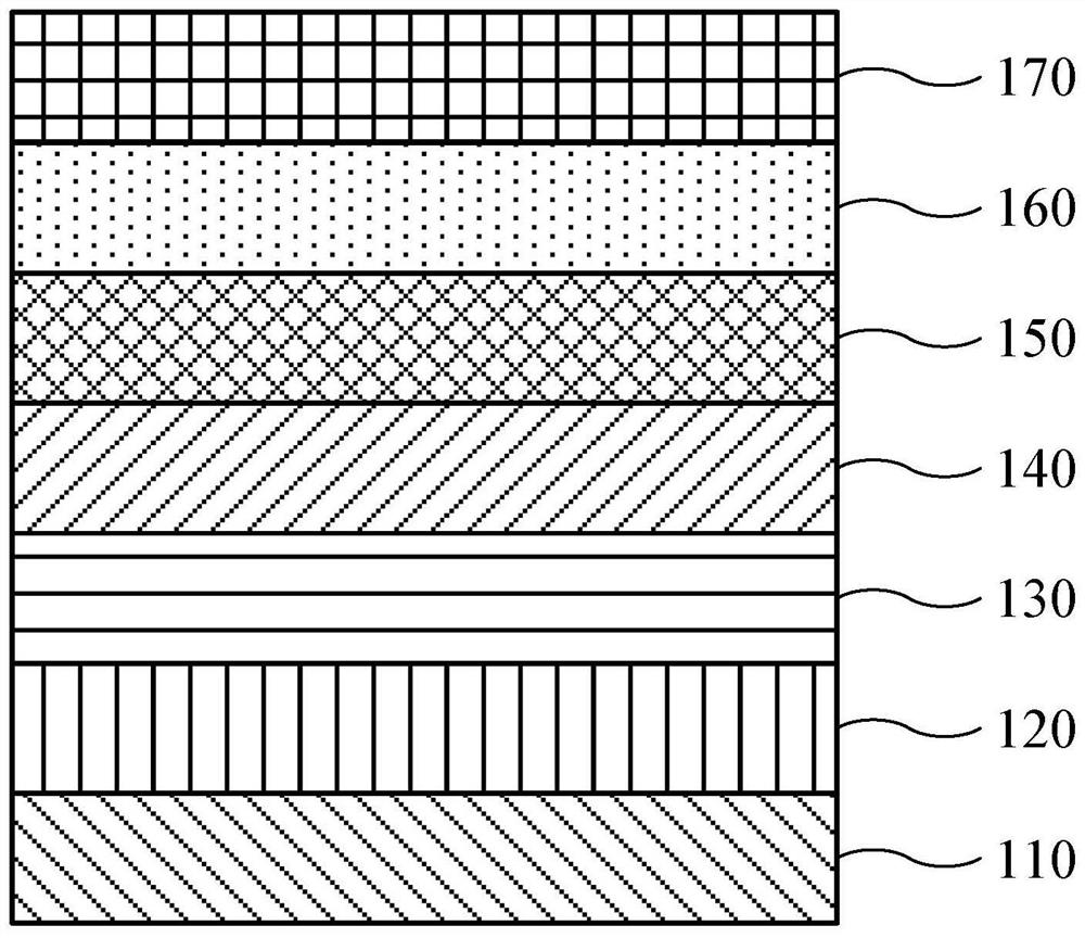
[0060] Step S1, preparing an anode on the substrate.

[0061] In a specific example, the material of the anode can be selected from silver, magnesium-silver alloy, gold, indium zinc oxide conductive film or indium tin oxide conductive film. The thickness of the anode 120 can be 20nm-100nm, for example, the thickness of the anode 120 is 20nm, 30nm, 40nm, 50nm, 60nm, 70nm, 80nm, 90nm, 100nm, or a range between the above thicknesses.

[0062] In a specific example, the substrate and the anode can be an integrated conductive glass, for example, glass is used as the substrate, and an indium tin oxide conductive film is used as the anode.

[0063] Step S2, depositing a hole injection layer on the anode.

[0064] In a specific example, the material of the hole injection layer is selected from materials with hole injection capability...

Embodiment 1

[0094] (1) Using transparent conductive film ITO as the anode, the thickness is 50nm;

[0095] (2) Deposit PEDOT by solution method on the anode: PSS is used as a hole injection layer with a thickness of 40nm;

[0096] (3) Utilizing solution method to deposit TFB on the hole injection layer as the hole transport layer, the thickness is 30nm;

[0097] (4) Deposit CdSe / ZnSe as a quantum dot luminescent layer on the hole transport layer by solution method, with a thickness of 15nm;

[0098] (5) Simultaneous deposition of SnO on the quantum dot light-emitting layer by solution method 2 Nanoparticles and HAT-CN as electron transport layer with a thickness of 50nm, in which HAT-CN and SnO 2 The mass ratio of 0.1:100;

[0099] (6) Depositing Ag as a cathode on the electron transport layer by evaporation method, with a thickness of 120 nm.

Embodiment 2

[0101] (1) Using transparent conductive film ITO as the anode, the thickness is 50nm;

[0102] (2) Deposit PEDOT by solution method on the anode: PSS is used as a hole injection layer with a thickness of 40nm;

[0103] (3) Utilizing solution method to deposit TFB on the hole injection layer as the hole transport layer, the thickness is 30nm;

[0104] (4) Deposit CdSe / ZnSe as a quantum dot luminescent layer on the hole transport layer by solution method, with a thickness of 15nm;

[0105] (5) Simultaneous deposition of SnO on the quantum dot light-emitting layer by solution method 2 Nanoparticles and HAT-CN as electron transport layer with a thickness of 50nm, in which HAT-CN and SnO 2 The mass ratio of 0.07:100;

[0106] (6) Depositing Ag as a cathode on the electron transport layer by evaporation method, with a thickness of 120 nm.


PUM

PropertyMeasurementUnit
Thicknessaaaaaaaaaa

Abstract

The invention discloses a composite material, an electroluminescent diode and a display device. The composite material comprises an electron transport material and an electron trap material which are mixed, the electron transport material is an n-type metal oxide, and the absolute value of the LUMO energy level of the electron trap material is 5-8 eV. Experiments prove that the n-type metal oxide material is doped with the electron trap material with the deep LUMO energy level to serve as the electron transport layer, the luminance rise range of the electroluminescent diode at the initial stage of light emitting is reduced or the luminance is slowly reduced at the initial stage of light emitting, and the luminance is not remarkably increased. In addition, the electroluminescent diode with the electron transport layer also has higher external quantum efficiency and more excellent service life performance.

Description

technical field [0001] The invention relates to the technical field of electronic display, in particular to a composite material, an electroluminescence diode and a display device. Background technique [0002] Electroluminescent diodes can directly convert electrical energy into light energy, and have been widely used in human daily production and life. Quantum dots have unique optical properties, such as continuously adjustable emission wavelength with size and composition, narrow emission spectrum, high fluorescence efficiency, and good stability. This has led to extensive attention and research on quantum dot-based electroluminescent diodes, and quantum dot light-emitting diodes are also considered to be the most promising next-generation display devices. [0003] The performance of quantum dot light-emitting diodes in traditional technologies has been significantly improved. The highest external quantum efficiency of red, green, and blue quantum dot light-emitting dio...

Claims


Application Information

Patent Timeline
IPC IPC(8): H01L51/50
CPCH10K50/11H10K2101/40H10K50/165H10K50/18
Inventor 苏亮
Owner GUANGDONG JUHUA PRINTING DISPLAY TECH CO LTD
Why Eureka
Try Eureka