Laser welding method and system for dissimilar metal film
A technology of laser welding and metal thin film, which is applied in the direction of laser welding equipment, welding equipment, welding equipment, etc., can solve problems such as difficult application, lack of strength, and poor forming, so as to improve the effect of welding process, reduce the bending caused by heat, Avoid the effect of false welding or over welding
- Summary
- Abstract
- Description
- Claims
- Application Information
AI Technical Summary
Problems solved by technology
Method used
Image
Examples
Embodiment 1
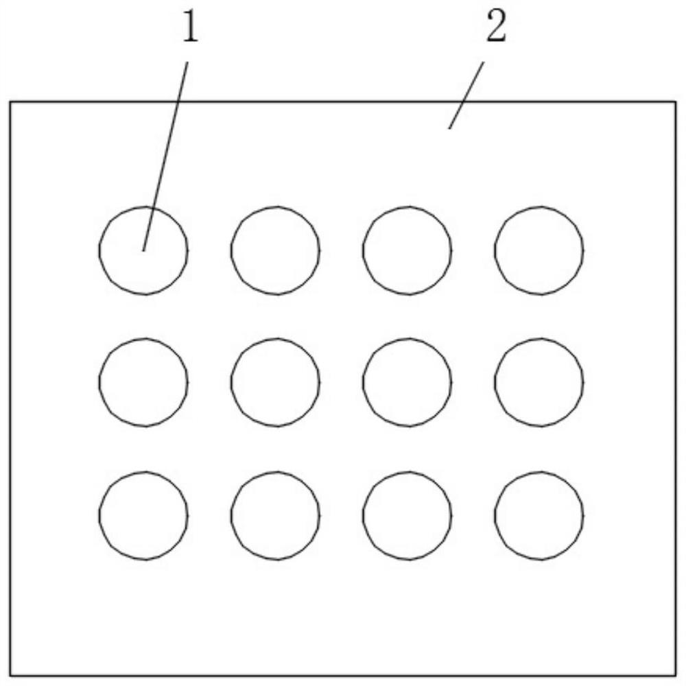
[0048] On the aluminum film 2, a plurality of circular solder joints arranged at intervals are formed with the copper film. Wherein, the thicknesses of the copper film and the aluminum film 2 are 20 μm and 80 μm respectively. The aluminum film has a length of 250 mm and a width of 200 mm, on which a plurality of copper solder joints 1 with a diameter of 4 mm arranged in an array need to be formed.
[0049] The steps are:
[0050] S1. Set the laser welding route according to the welding shape and area of the copper film and the aluminum film.
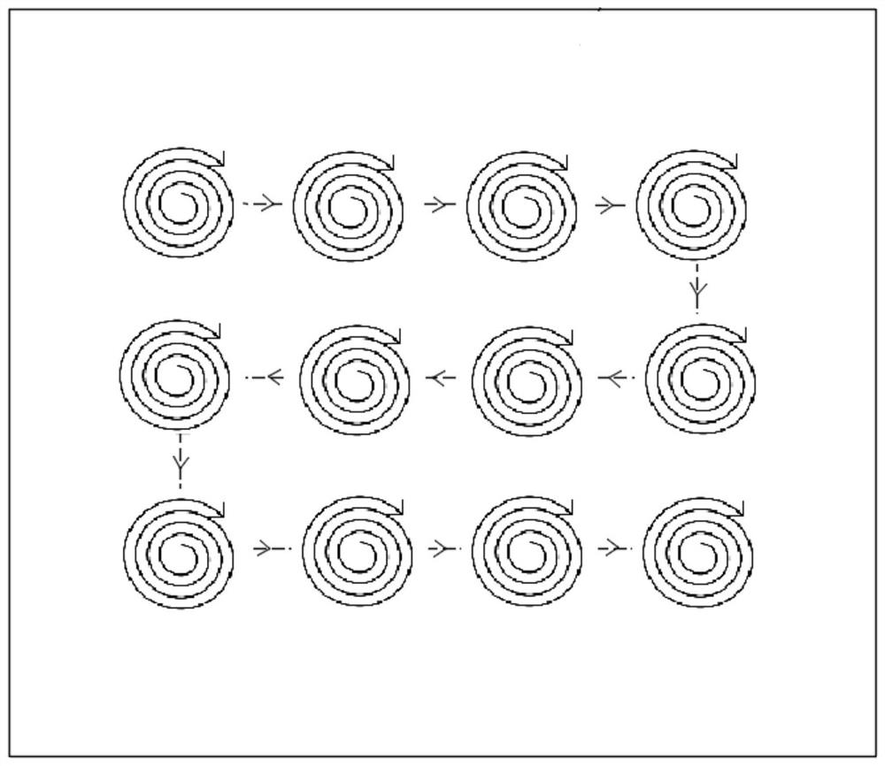
[0051] The welding route of a solder joint is a spiral welding route from inside to outside or from outside to inside, such as figure 2 As shown, the minimum diameter is between 0.5-1.5mm, the maximum diameter is 4mm, and the distance between adjacent helixes is 0.1-0.5mm.
[0052] After a solder spot is welded, jump to other solder spots for welding, such as image 3 As shown, in this embodiment, jump to adjacent welding spots fo...
Embodiment 2
[0063] The principle, method and structure of this embodiment are basically the same as those of Embodiment 1, the difference is that, as Figure 4 with Figure 5 As shown, the copper solder joint 1 is a square solder joint with a side length of 4 mm. The welding path of a single spot, as a square helix.
Embodiment 3
[0065] The principle, method and structure of this embodiment are basically the same as those of Embodiment 1, the difference is that, as Image 6 As shown, the entire copper film is soldered on the aluminum film. Its solder joints are set as circular solder joints set in an array. The solder joint size is 4mm, the distance between adjacent solder joints is 27mm, and the distance from the edge of the outermost solder joint to the edge of the copper film is 13.875mm.
[0066] S4 When cutting the excess copper film, it can be cut according to the outer edge of the aluminum film. Effect picture as Figure 7 shown.
PUM
| Property | Measurement | Unit |
|---|---|---|
| Thickness | aaaaa | aaaaa |
| Thickness | aaaaa | aaaaa |
| Length | aaaaa | aaaaa |
Abstract
Description
Claims
Application Information


