Preparation method of semiconductor memory, and semiconductor memory

A semiconductor and memory technology, applied in the fields of semiconductor/solid-state device manufacturing, semiconductor devices, electric solid-state devices, etc., can solve problems such as difficult control and complex process, and achieve the effect of reducing manufacturing cost, saving manufacturing process and improving manufacturing efficiency

Pending Publication Date: 2022-02-22
CHANGXIN MEMORY TECH INC
View PDF10 Cites 0 Cited by
  • Summary
  • Abstract
  • Description
  • Claims
  • Application Information

AI Technical Summary

Problems solved by technology

In this way, the bottom of the Cell needs to be aligned with the storage node pad, the storage node pad and the storage node, and the storage node and the active area. The process is complex and difficult to control.

Method used


Image

  • Preparation method of semiconductor memory, and semiconductor memory
  • Preparation method of semiconductor memory, and semiconductor memory
  • Preparation method of semiconductor memory, and semiconductor memory

Examples


preparation example Construction

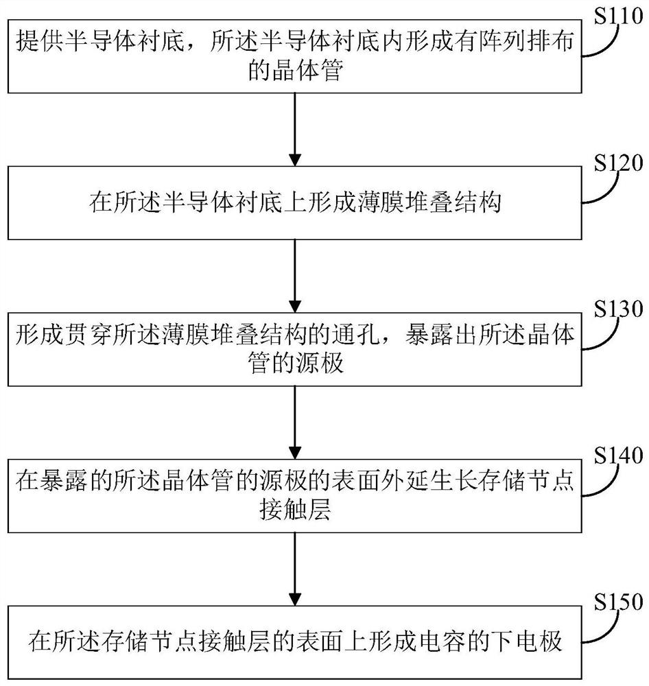
[0039] figure 1 A flow chart of a method for manufacturing a semiconductor memory according to an embodiment of the present disclosure is schematically shown. Such as figure 1 As shown, the method provided by the embodiment of the present disclosure may include the following steps.

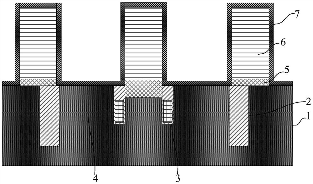
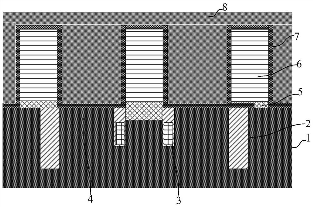
[0040] In step S110, a semiconductor substrate is provided, and transistors arranged in an array are formed in the semiconductor substrate.

[0041] Embodiments of the present disclosure provide a semiconductor substrate, which can be used to provide an operating platform for subsequent processes. The semiconductor substrate can be any substrate used to carry the components of the semiconductor integrated circuit, which can be a bare chip or a wafer processed by an epitaxial growth process. The semiconductor substrate may be, for example, a silicon-on-insulator (SOI) substrate, a bulk silicon (bulk silicon) substrate, a germanium substrate, a silicon germanium substrate, an indium phosphide (In...


PUM


Abstract

The invention relates to a preparation method of a semiconductor memory, and the semiconductor memory, and relates to the technical field of semiconductors. The method comprises the following steps: providing a semiconductor substrate, and forming transistors arranged in an array mode in the semiconductor substrate; forming a thin film stacking structure on the semiconductor substrate; forming a through hole penetrating through the thin film stacking structure, and exposing a source electrode of the transistor; epitaxially growing a storage node contact layer on the exposed surface of the source electrode of the transistor; and forming a lower electrode of a capacitor on the surface of the storage node contact layer. According to the scheme provided by the embodiment of the invention, the source electrode of the transistor is directly exposed by enabling the through hole to penetrate through the thin film stacking structure, and only one-time photomask alignment of the storage unit and the active region is needed, so that a large number of preparation processes can be saved.

Description

technical field [0001] The present disclosure relates to the technical field of semiconductors, and in particular, to a method for manufacturing a semiconductor memory and the semiconductor memory. Background technique [0002] A storage cell (Storage Cell, hereinafter referred to as Cell) in a semiconductor memory such as DRAM (Dynamic Random Access Memory, Dynamic Random Access Memory) uses a storage capacitor (Storage Capacitor, hereinafter referred to as capacitor) to store bit (Bit) information. From a theoretical point of view, the simplest DRAM Storage Cell that stores a Bit of information includes the following four parts: Storage Capacitor, which uses the amount of charge stored in it, or the sum of the voltage difference between the two ends of the capacitor Low, to represent logical 1 and 0; Transistor, the transistor, its on and off, determines whether to allow or prohibit the reading and rewriting of the information stored in the Storage Capacitor; Wordline, the...

Claims


Application Information

Patent Timeline
IPC IPC(8): H01L21/8242H01L27/108
CPCH10B12/31H10B12/033H10B12/0335H10B12/315H10B12/482H10B12/485
Inventor 张魁应战
Owner CHANGXIN MEMORY TECH INC
Why Eureka
Try Eureka