A maskless fabrication method for multilayer film capacitors

A multi-layer film and capacitor technology, applied in the direction of film/thick film capacitors, multilayer capacitors, fixed capacitor electrodes, etc., can solve the problems of high process control requirements, high cost, low efficiency, etc., and reduce the production process and cost. Low, simple process control effect

Active Publication Date: 2018-10-12
GUILIN UNIV OF ELECTRONIC TECH
View PDF5 Cites 0 Cited by
  • Summary
  • Abstract
  • Description
  • Claims
  • Application Information

AI Technical Summary

Problems solved by technology

[0003] For thin-film components, especially multi-layer film capacitors, in the process of electrode film patterning, if traditional photolithography technology is used, each layer of electrodes needs to be patterned, and facing the production of hundreds or thousands of layers Process requirements, high cost, and low efficiency are still difficult to break through; physical mask technology requires high mask plate and alignment accuracy, and requires high process control for micro-sized MLCC products, which is difficult to meet practical application requirements

Method used


Image

  • A maskless fabrication method for multilayer film capacitors
  • A maskless fabrication method for multilayer film capacitors
  • A maskless fabrication method for multilayer film capacitors

Examples


Embodiment 1

[0032] Such as the above-mentioned invention patent, the specific implementation steps are as follows:

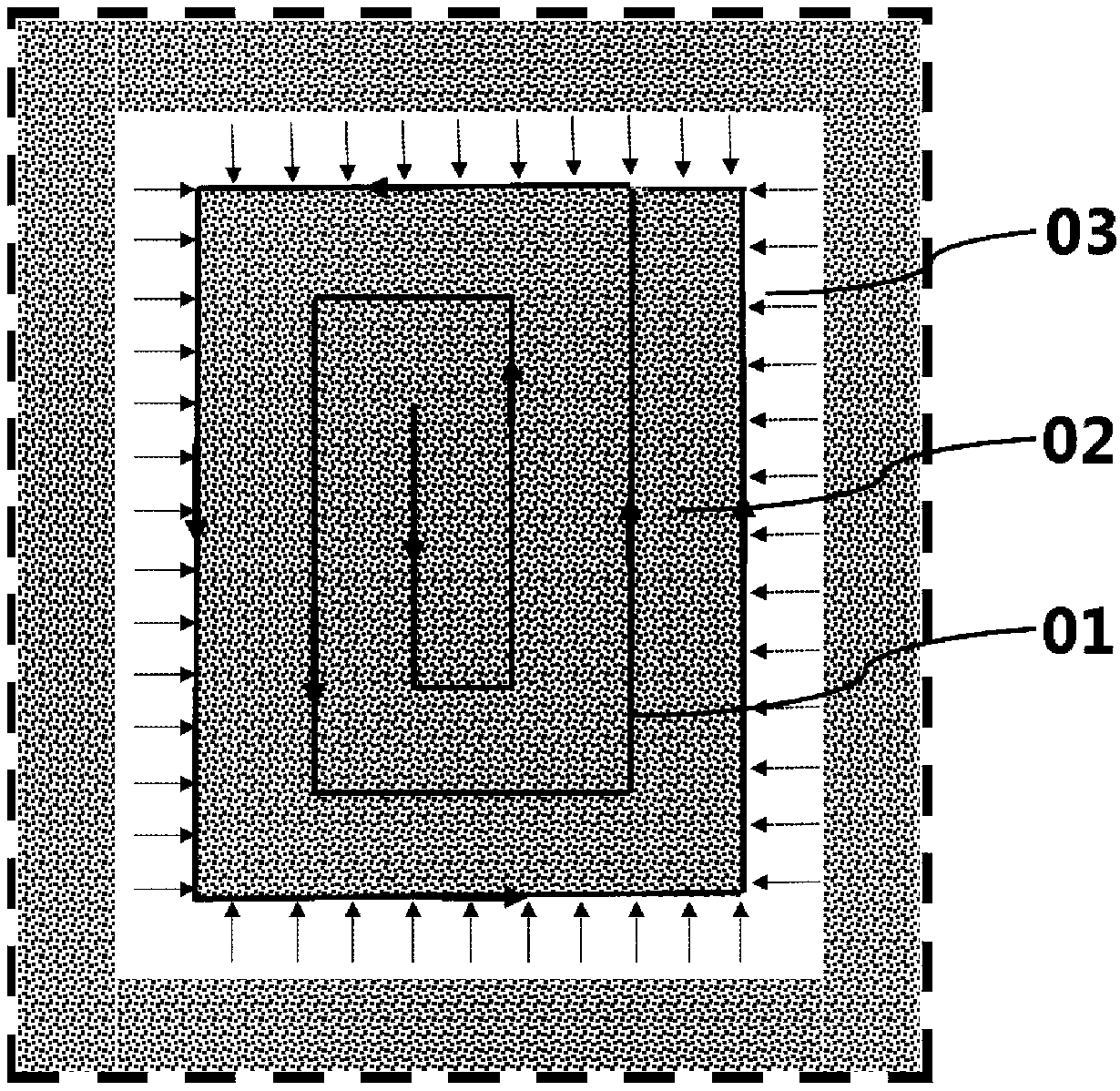
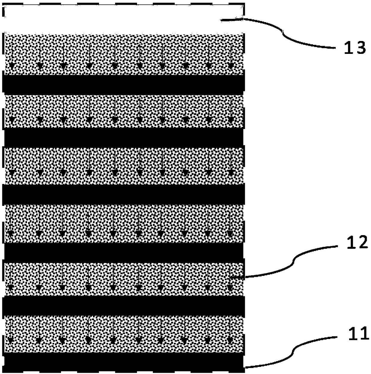
[0033] (1) The metal Ag powder with an average particle size of 50nm is prepared into a slurry according to metal powder: epoxy resin = 50:50 (mass percentage), and then the electrode layer with a thickness of 200nm is prepared on the alumina ceramic substrate, Then, a square infrared spot with a side length of 0.05 mm at 90°C was used to press the figure 1 The method shown is to carry out directional scanning heating on the surface of the film. The length and width of the directional scanning heating area are 0.2×0.1 mm. Finally, a laser beam with a temperature of 550 ° C, a line width of 30 μm, and a length of 0.1 mm is used to press the figure 2 In the shown manner, the thin film is heated directionally, and finally the metal electrode is formed into the desired electrode pattern.

[0034] (2) Using butyl titanate, barium acetate, glacial acetic acid and acetylacetone ...

Embodiment 2

[0038] (1) The metal Ni powder with an average particle size of 20nm is prepared into a slurry according to metal powder: epoxy resin = 60:40 (mass percentage), and then an electrode layer with a thickness of 100nm is prepared on a quartz substrate, and then A circular infrared spot with a diameter of 0.03mm at 50°C is used to press the figure 1 The method shown is to carry out directional scanning heating on the surface of the film. The length and width of the directional scanning heating area are 0.4×0.2 mm. Finally, a laser beam with a temperature of 450 ° C, a line width of 10 μm, and a length of 0.2 mm is used to press figure 2 In the shown manner, the thin film is heated directionally, and finally the metal electrode is formed into the desired electrode pattern.

[0039] (2) Using butyl titanate, barium acetate, glacial acetic acid, acetylacetone, zirconium acetate and other raw materials according to the ratio of Y5V porcelain powder, prepare a sol with a metal ion dep...

Embodiment 3

[0043](1) The metal Cu powder with an average particle size of 200nm was prepared into a slurry according to metal powder: epoxy resin = 65:35 (mass percentage), and then the electrode layer with a thickness of 500nm was prepared on a silicon wafer, and then A circular infrared spot with a diameter of 0.05mm at 150°C is used to press the figure 1 The method shown is for directional scanning heating on the surface of the film. The length and width of the directional scanning heating zone are 0.6×0.3. figure 2 In the shown manner, the thin film is heated directionally, and finally the metal electrode is formed into the desired electrode pattern.

[0044] (2) Using butyl titanate, barium acetate, glacial acetic acid, acetylacetone, zirconium acetate and other raw materials according to the ratio of Y5V porcelain powder, prepare a sol with a metal ion depth of 0.2mol / L, and prepare it on the above patterned electrode substrate through several A Y5V dielectric film with a thickne...


PUM

PropertyMeasurementUnit
particle sizeaaaaaaaaaa
thicknessaaaaaaaaaa
thicknessaaaaaaaaaa

Abstract

The invention discloses a maskless preparation method of a multi-layer thin-film capacitor. According to the method, firstly, nano metal powder slurry is prepared or non-metallic conductive oxide colloid is prepared by a sol-gel method; a substrate is evenly coated with the nano metal powder slurry or the non-metallic conductive oxide colloid; directional scanning and heating are carried out on the substrate through an infrared spot with controlled temperature, so that the slurry or the colloid is subjected to directional shrinkage in the drying and volatilizing processes and forms an initial electrode pattern; the surface of a metal electrode material is bonded or the non-metallic conductive oxide is crystallized by laser spot heating and a clear electrode pattern is formed; finally a dielectric film is prepared by the sol-gel method or a sputtering method; an electrode film is prepared on the dielectric film according to the method; a staggered layer is formed by the second layer of electrode and the bottom electrode by directional scanning and heating; and the steps are repeated to prepare the multi-layer thin-film capacitor with an interdigital structure. According to the maskless preparation method, preparation of the multi-layer thin-film capacitor can be realized without a mask or a photolithography; and the maskless preparation method has the characteristics of being low in cost and simple in process control.

Description

technical field [0001] The invention belongs to the technical field of thin film component preparation, and relates to a maskless preparation method of a multilayer thin film capacitor, in particular to a method for directionally heating colloid with infrared light spots and directional shrinking of the colloid to achieve electrode film patterning. Background technique [0002] With the miniaturization and high-capacity development of electronic components, especially multilayer ceramic capacitors (MLCC), for example, the size of advanced MLCC products has grown to 01005 size, and the traditional thick-film method of manufacturing MLCC has been affected by materials, pastes, Due to the many limitations of screen printing technology, it is difficult to meet the needs of further miniaturization of MLCC components. Semiconductor thin film technology has become one of the main development directions for manufacturing micro-miniature electronic components. However, due to the in...

Claims


Application Information

Patent Timeline
Patent Type & Authority Patents(China)
IPC IPC(8): H01G4/005H01G4/228H01G4/008H01G4/33
Inventor 徐华蕊朱归胜
Owner GUILIN UNIV OF ELECTRONIC TECH
Why Eureka
Try Eureka