
Silicon carbide single crystal and growth device and preparation method thereof

A silicon carbide single crystal and growth device technology, applied in the direction of single crystal growth, single crystal growth, chemical instruments and methods, etc., can solve problems such as the appearance of large steps at the interface, stacking fault polytype inclusions, etc., and achieve reduction Defects, avoid condensation, inhibit growth effects

Active Publication Date: 2022-02-25
江苏集芯半导体硅材料研究院有限公司
View PDF6 Cites 0 Cited by
  • Summary
  • Abstract
  • Description
  • Claims
  • Application Information

AI Technical Summary

Problems solved by technology

The traditional PVT method is affected by the uneven gas phase transmission in the process of growing silicon carbide single crystal, so that the interface of the grown silicon carbide single crystal is mostly a convex interface, which will lead to the appearance of coarse steps, stacking faults, Inclusions of exotic polytypes and other defects
[0004] Therefore, the existing technology for preparing silicon carbide single crystal needs to be improved

Method used


Image

  • Silicon carbide single crystal and growth device and preparation method thereof
  • Silicon carbide single crystal and growth device and preparation method thereof
  • Silicon carbide single crystal and growth device and preparation method thereof

Examples


Embodiment 1

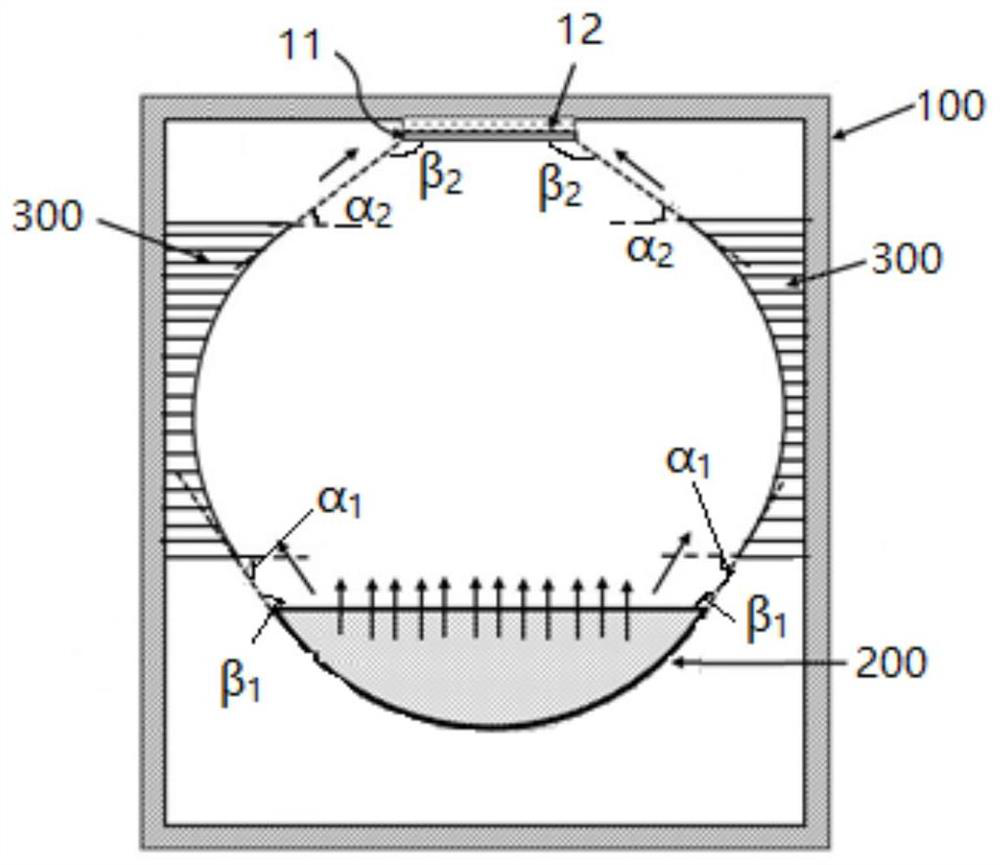
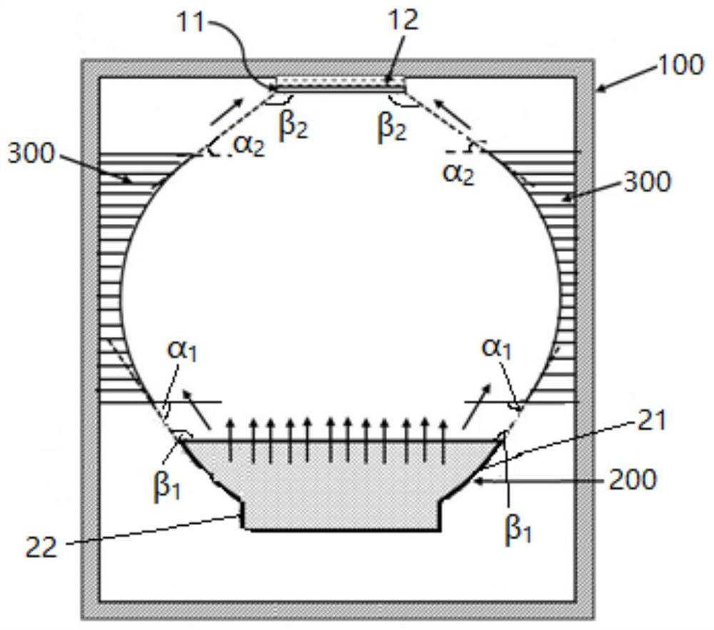
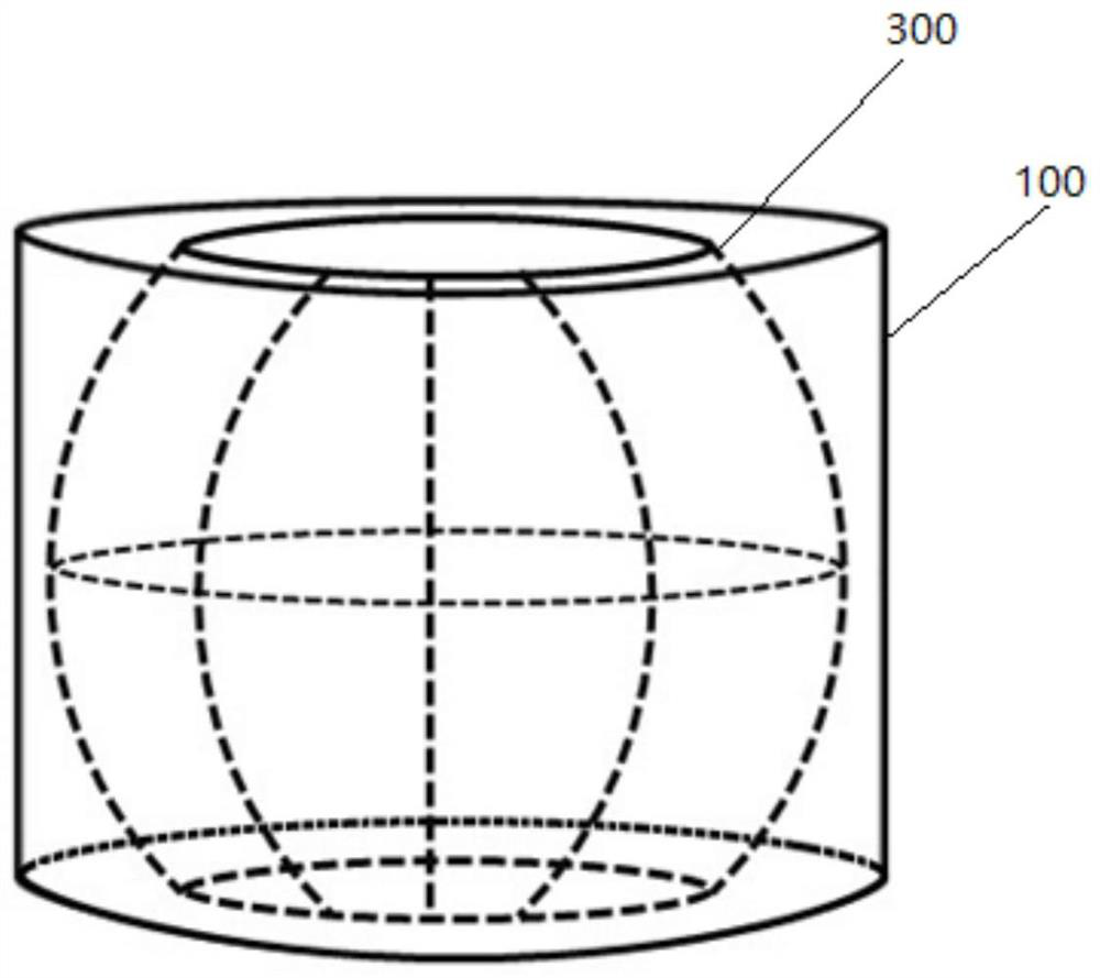
[0072] refer to Figure 5 , The silicon carbide single crystal growth device comprises a growth crucible 100, an inner crucible 200 (made of graphite), a guide tube 300 (made of graphite), an inner crucible base 400 (made of graphite) and a rotating shaft 500 (made of graphite) , the inner crucible 200 adopts a pot-like wide-caliber, the seed crystal 11 is fixed on the top center of the growth crucible 100 through the seed crystal base 12, silicon carbide powder is placed in the inner crucible 200, and the outer wall of the inner crucible 200 is close to and fixed on On the inner wall of the inner crucible base 400, the guide tube 300 is arranged between the seed crystal 11 and the inner crucible 200 and surrounds the inner wall of the growth crucible 100, and the inner wall of the guide tube 300 is in the shape of a smooth arc, and the inner crucible 200 and the guide The flow tube 300 cooperates to form a gas transmission and drainage channel, the tangent line of the lower e...

Embodiment 2

[0074] refer to Image 6 , the inner crucible 200 is adopted from top to bottom and includes a reduced diameter portion 21 and an equal diameter portion 22, and the rest are the same as in Embodiment 1.


PUM


Abstract

The invention discloses a silicon carbide single crystal and a growth device and a preparation method thereof. The growth device of the silicon carbide single crystal comprises a growth crucible, an inner crucible and a flow guide cylinder. A seed crystal is arranged at the top of the growth crucible. The inner crucible is positioned at the bottom in the growth crucible, and the cross sectional area of the inner crucible is reduced from top to bottom. The flow guide cylinder is arranged in the growth crucible and located between the inner crucible and the seed crystal, the flow guide cylinder is arranged around the inner wall of the growth crucible, the inner wall of the flow guide cylinder is in an arc shape, and the inner crucible and the flow guide cylinder are matched to form a gas transmission drainage channel. Therefore, by adopting the growth device, the edge defect of a silicon carbide single crystal can be effectively improved, so that a high-quality silicon carbide single crystal is obtained.

Description

technical field [0001] The invention belongs to the field of single crystals, and in particular relates to a silicon carbide single crystal, a growth device and a preparation method thereof. Background technique [0002] Silicon carbide (SiC) single crystal material is a relatively mature wide-bandgap semiconductor material, which is widely used in high-voltage, high-frequency, high-power and high-temperature-resistant fields. At present, the proportion of silicon carbide power devices used in new energy vehicles, photovoltaic inverters, rail transit, UHV power grids and 5G communications is increasing year by year. In the near future, silicon carbide single crystal materials will become one of the most important electronic materials. [0003] The most commonly used method for growing SiC single crystals is Physical Vapor Transport (PVT), which involves placing high-purity SiC powder and seed crystals on the bottom and top of a graphite crucible, respectively, and heating t...

Claims


Application Information

Patent Timeline
IPC IPC(8): C30B23/02C30B29/36
CPCC30B23/02C30B29/36
Inventor 燕靖陈俊宏吴亚娟
Owner 江苏集芯半导体硅材料研究院有限公司
Learn More