Piezoresistive pressure sensor and preparation method thereof
A pressure sensor and piezoresistive technology, applied in the field of piezoresistive pressure sensor and its preparation, can solve the problems of high sensitivity of flat membrane structure, insufficient structural strength, poor resistance to vibration, etc., and achieve the improvement of insufficient strength, flexible style and sensitivity. improved effect
- Summary
- Abstract
- Description
- Claims
- Application Information
AI Technical Summary
Problems solved by technology
Method used
Image
Examples
Embodiment 1
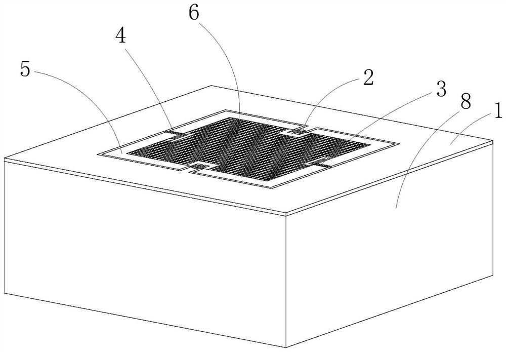
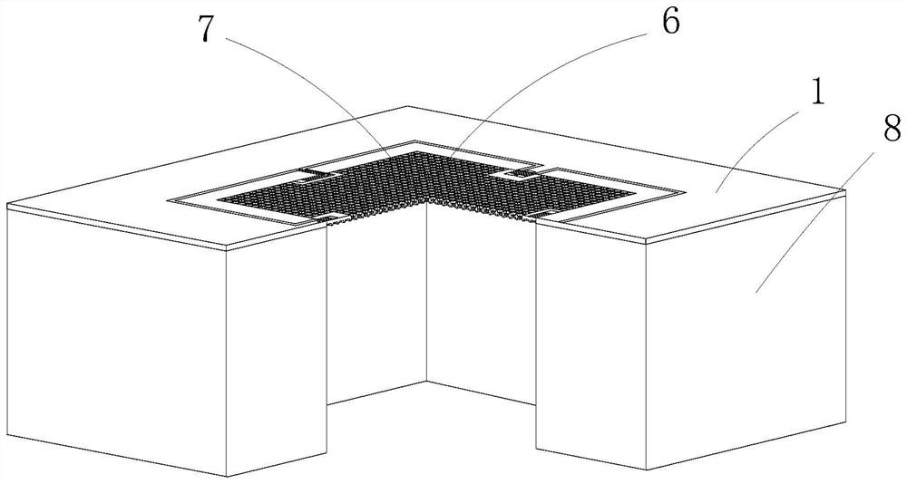
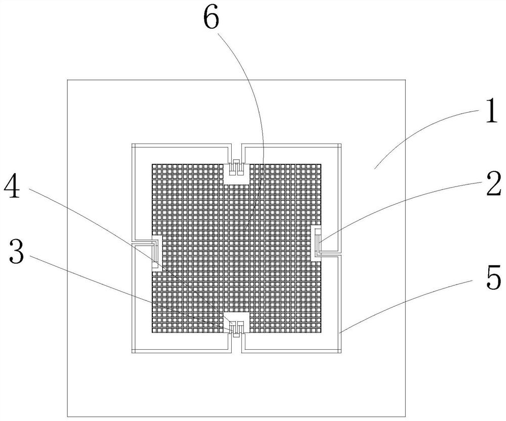
[0042] Such as Figure 1-5 As shown, the embodiment of the present invention is provided with a dielectric pressure sensor, including silicon strain films 1, a pressure sensitive resistor strip 2, a heavy doped contact zone 3, an electrode aperture 4, a metal lead 5, and a glass base 8. The silicon strain diaphragm 1 is a silicon wafer to form a silicon wafer to form a honeycomb structure after electrical etching and back etch etching, including four groups, respectively, respectively in silicon strain film 1, respectively. In the middle of the top layer, the metal lead 5 and the heavier contact zone 3 form ohmic contact through the electrode hole 4 on the front side of the silicon strain film 1, which is used for bonding silicon strain film 1.
[0043] Such as Figure 1-5 As shown, the silicon strain film 1 is an N-type silicon-on-insulator silicon wafer.
[0044] Further, the honeycomb structure includes a front groove and a back groove comprising a plurality of, uniformly arrang...
Embodiment 2
[0049] A method of preparing a MEMS dielectric pressure sensor, the steps include:
[0050] S1: Made in the front of the silicon-stranded diaphragm 1, a mutually connected varistor strip and a heavy doped contact area;
[0051] S2: Making lead holes and metal leads on the front surface of the silicon strain diaphragm;
[0052] S3: Ette the front groove in front of the silicon-strained diaphragm;
[0053] S4: etching the back groove corresponding to the front groove on the back photolithography of the silicon-strain diaphragm;
[0054] S5: Remove the back groove to a suitable size;
[0055]S6: The silicon-stranded diaphragm obtained by the honeycomb structure obtained by step S5 is bonded to a hole or a cavity of the glass base bonded to the pressure sensor.
[0056] Further, according to step S1, a pressure sensitive resistor strip and a heavily doped contact zone are produced by ion implantation.
[0057] Further, according to step S2, the metal lead is made of aluminum, chromium...
PUM
 Abstract
Description
Claims
Application Information


