Transparent broadband electromagnetic wave absorber based on ITO resistive film

A technology of wave absorber and resistive film, which is applied in the field of transparent broadband electromagnetic wave absorber, can solve the problems of slowly overcoming, sensitivity, and incident electromagnetic wave polarization-sensitive incident angle, so as to reduce thickness and weight, expand application range, The effect of good light transmission performance

Active Publication Date: 2022-03-01
NANJING UNIV OF AERONAUTICS & ASTRONAUTICS
View PDF7 Cites 3 Cited by
  • Summary
  • Abstract
  • Description
  • Claims
  • Application Information

AI Technical Summary

Problems solved by technology

With the emergence of transparent absorbers, various transparent electromagnetic absorbers with new structures have been proposed one after another, and their functions and performance have also been improved, from the initial absorption of single-frequency incident electromagnetic waves to the gradual design of Electromagnetic absorbers with dual frequency points, multi-frequency points, and wide frequency bands can be realized, and the absorber initially has the disadvantages of being sensitive to the polarization and angle of incidence of incident electromagnetic waves, but with the subsequent structural optimization design, it slows down. slow to overcome these deficiencies

Method used


Image

  • Transparent broadband electromagnetic wave absorber based on ITO resistive film
  • Transparent broadband electromagnetic wave absorber based on ITO resistive film
  • Transparent broadband electromagnetic wave absorber based on ITO resistive film

Examples


Embodiment Construction

[0022] Below in conjunction with accompanying drawing and specific embodiment the present invention is described in further detail:

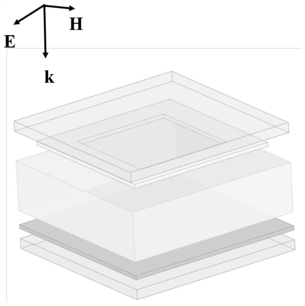
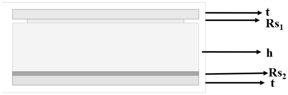
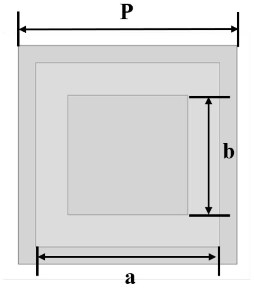
[0023] Such as figure 1 , figure 2 As shown, a transparent broadband electromagnetic absorber based on an ITO resistive film, including a first dielectric layer, a conductive film, a second dielectric layer, a resistive film, and a third dielectric layer from bottom to top, wherein the resistive film adopts magnetic sputtering It is printed on the lower surface of the third dielectric layer by magnetic sputtering technology, and several square ring units are arranged periodically. The conductive film is also printed on the upper surface of the first dielectric layer by magnetic sputtering technology, and the conductive film completely covers the first dielectric layer. the upper surface of the dielectric layer. Concrete structural parameters in this embodiment are as figure 2 and image 3 Shown: the thickness of the dielectric layer t=0.55...


PUM

PropertyMeasurementUnit
thicknessaaaaaaaaaa
thicknessaaaaaaaaaa
widthaaaaaaaaaa

Abstract

The invention discloses a transparent broadband electromagnetic wave absorber based on an ITO resistive film, which belongs to the technical field of electromagnetic materials and comprises an upper glass substrate, a lower glass substrate, ITO periodic units etched on the two glass substrates and having different sheet resistance values, and a middle transparent glass substrate, the periodic unit structure is a square ring patch, and the square ring patch is a layer of thin film formed by etching ITO with square resistance on a glass substrate. The middle layer selects glass for impedance matching to achieve the purpose of transparency, ITO with sheet resistance is completely etched on the bottom layer glass substrate, and the bottom layer ITO can be regarded as a metal reflecting plate due to the fact that the sheet resistance of the bottom layer ITO is very small, and the conductivity of the bottom layer ITO is close to that of a perfect metal conductor. The wave absorber realized by the resistive ITO and the glass breaks through the limitation that the traditional wave absorber is opaque and narrow in bandwidth, the application scene is widened, and the wave absorber has important application prospects in the aspects of electromagnetic shielding, cockpits with requirements on light transmittance and the like.

Description

technical field [0001] The invention belongs to the technical field of electromagnetic materials, and in particular relates to a transparent broadband electromagnetic wave absorber based on an ITO resistance film. Background technique [0002] Electromagnetic absorber (EMA) is an important electromagnetic device, which plays a very important role in the fields of electromagnetic compatibility, electromagnetic stealth, and information security. With the rapid development of science and technology, various electronic components produce a large amount of electromagnetic radiation of different frequencies, which puts forward higher requirements for the performance, size, angular stability and other indicators of the absorber. EMA has been increasingly widely used due to its advantages such as high absorption rate and flexible design. [0003] The prototype of the EMA was first proposed by the American researcher Winfield Salisbury in 1952, the SalisburyScreen, which consists of...

Claims


Application Information

Patent Timeline
Patent Type & Authority Applications(China)
IPC IPC(8): H01Q17/00
CPCH01Q17/008
Inventor 胡雪容王毅曹群生吴祯夏雨
Owner NANJING UNIV OF AERONAUTICS & ASTRONAUTICS
Why Eureka
Try Eureka