Preparation method of refrigeration-free anti-reflection InP-based quantum dot/quantum well coupled EML epitaxial wafer

A quantum well and quantum-based technology, which is applied in the direction of phonon exciters, the structure of optical resonators, laser components, etc., can solve the problems of increasing device cost and complexity, and achieve wide applicability, good effect, and strong practicality sexual effect

Pending Publication Date: 2022-03-15
JIANGSU HUAXING LASER TECH CO LTD
View PDF7 Cites 2 Cited by
  • Summary
  • Abstract
  • Description
  • Claims
  • Application Information

AI Technical Summary

Problems solved by technology

Therefore, optical isolators need to be introduced in the device to reduce optical feedback, which increases the cost and complexity of the device

Method used


Image

  • Preparation method of refrigeration-free anti-reflection InP-based quantum dot/quantum well coupled EML epitaxial wafer
  • Preparation method of refrigeration-free anti-reflection InP-based quantum dot/quantum well coupled EML epitaxial wafer
  • Preparation method of refrigeration-free anti-reflection InP-based quantum dot/quantum well coupled EML epitaxial wafer

Examples


Embodiment

[0045] A method for preparing an anti-reflection InP-based quantum dot / quantum well coupled EML epitaxial wafer without refrigeration, comprising the following steps:

[0046] Step 1. Select InP substrate A: the substrate is n + Type indium phosphide single wafer, crystal orientation is (100), doped element Si, doping concentration is (1-3)×10 18 cm -3 .

[0047] Step 2, performing the first epitaxial growth of the quantum dot stack on the InP substrate A; the epitaxial growth methods include molecular beam epitaxy and metal organic chemical deposition.

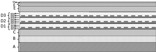
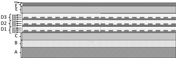
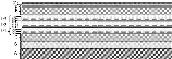
[0048] The structure grown for the first time is InP buffer layer B, InGaAsP lower confinement layer C, InAs / InGaAsP quantum dot active layer, InGaAsP upper confinement layer E, InGaAsP Gallium arsenide phosphorous grating layer F and indium phosphide capping layer G1, the structure is as follows figure 1 shown.

[0049] Wherein, the thickness of the indium phosphide buffer layer (B) is 500nm;

[0050] The thickness of th...


PUM

PropertyMeasurementUnit
grating periodaaaaaaaaaa
thicknessaaaaaaaaaa
thicknessaaaaaaaaaa

Abstract

According to the preparation method of the refrigeration-free anti-reflection InP-based quantum dot / quantum well coupling EML epitaxial wafer, a quantum well electric absorption modulation region which is covered by an ohmic contact layer and is horizontally coupled with a quantum dot stacking region is additionally arranged in the quantum dot stacking region in a quantum dot laser based on an InP substrate. The electro-absorption modulated laser is prepared through molecular beam epitaxy or metal organic chemical vapor deposition and is formed by integrally growing a quantum dot distributed feedback laser and a quantum well electro-absorption modulator in a butt-joint growth mode; the electro-absorption modulated laser combines the characteristics of excellent reflection resistance and high temperature stability of a quantum dot laser and the characteristic of high modulation rate of a quantum well electro-absorption modulator, and realizes stable work at 5-75 DEG C under the conditions of no optical isolator and no refrigeration. The preparation method is clear and simple in steps and easy to operate, and the prepared electro-absorption modulated laser is good in effect, stable in performance, capable of working continuously, high in practicability and wide in applicability.

Description

technical field [0001] The invention relates to a preparation method of a laser epitaxial wafer, in particular to a preparation method of an uncooled anti-reflection InP-based quantum dot / quantum well coupled EML epitaxial wafer, and belongs to the technical field of semiconductors. Background technique [0002] Semiconductor laser is an electro-optical conversion device that converts electrical signals into optical signals. According to the different modulation methods of electrical signals, it is divided into two types: direct modulation laser (DML) and external modulation laser. Direct modulation refers to directly injecting the current of an additional high-frequency electrical signal into the semiconductor laser to realize the modulation of the optical signal, and the external modulation is to use a Mach-Zehnder (MZ) modulator or an electro-absorption (EA) ) The modulator modulates the output laser. The direct modulation method of the laser is the simplest and easy to ...

Claims


Application Information

Patent Timeline
Patent Type & Authority Applications(China)
IPC IPC(8): H01S5/343H01S5/12
CPCH01S5/343H01S5/12
Inventor 王岩徐鹏飞罗帅季海铭
Owner JIANGSU HUAXING LASER TECH CO LTD
Why Eureka
Try Eureka