Forming method of semi-embedded thick copper fine circuit of flexible packaging substrate

A flexible packaging and fine circuit technology, applied in chemical/electrolytic methods to remove conductive materials, printed circuits, printed circuit manufacturing, etc., can solve the difficulty in controlling the shape of copper-plated circuits, the decline in the exposure resolution of photosensitive materials, and affect product quality and other problems, to achieve the effect of easy ink overflow precision control, reduce the occurrence of line peeling, and small ink capillary effect

Pending Publication Date: 2022-03-15
LEADER TECH ELECTRONICS SHENZHEN INC
View PDF12 Cites 0 Cited by
  • Summary
  • Abstract
  • Description
  • Claims
  • Application Information

AI Technical Summary

Problems solved by technology

[0005] The principle of the semi-additive method for circuit forming has the following defects: 1. The cross-sectional shape of the circuit using the semi-additive method is determined by the photosensitive material cross-section after development, and the thickness of the copper-plated circuit exceeds the surface of the photosensitive material. Control, so the copper thickness of the line is limited by the thickness of the photosensitive material
However, when the photosensitive material becomes thicker, the exposure resolution of the photosensitive material will decrease, which cannot meet the forming requirements of fine lines.
Therefore, the thickness of photosensitive materials generally needs to be controlled at 3 to 5 microns, and the copper thickness of fine lines is generally controlled at about 6 to 8 microns, which cannot form a thick copper line that meets the heat dissipation capability of the chip, so its heat dissipation performance is difficult to improve
2. When the semi-additive circuit is formed, the nickel-chromium seed layer needs to be etched after copper plating, and the thickness of the copper-plated circuit part will also be etched and thinned synchronously, which will affect the copper thickness of the circuit.
3. When the semi-additive method is used to etch the seed layer, the etching will be unclean, resulting in defects such as short circuit and short circuit of the product, which will affect the quality of the product
However, if the conventional semi-additive method uses a polyimide material with a thickness that is too thin, it will cause the product to wrinkle more easily during the transportation process. Therefore, the polyimide film material with a thickness of more than 34 microns is currently used in the industry. limits the further development of its heat dissipation capability
5. In the circuit structure of the semi-additive method, only the bottom surface of the circuit is combined with the polyimide material, and its bonding force is poor, and it is easy to cause poor copper circuit peeling.

Method used


Image

  • Forming method of semi-embedded thick copper fine circuit of flexible packaging substrate
  • Forming method of semi-embedded thick copper fine circuit of flexible packaging substrate
  • Forming method of semi-embedded thick copper fine circuit of flexible packaging substrate

Examples


Embodiment Construction

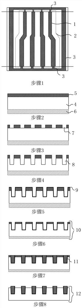
[0034] like figure 1 A method for forming a semi-embedded thick copper fine circuit of a flexible packaging substrate is characterized in that it includes the steps:

[0035] Step 1: In the product design stage, connect the product line 1 to the electroplating wire 3 outside the product outline line 2 to realize electrical conduction during copper electroplating;

[0036] Step 2: Coating a layer of photosensitive material I5 on the upper surface of the polyimide film 4, laminating a layer of photosensitive material II6 on the lower surface of the polyimide film 4;

[0037] Step 3: Exposing the photosensitive material I5 on the upper surface, transferring the circuit pattern to the photosensitive material I5, and developing 7 after the exposure is completed, that is, using the developer to remove the photosensitive material I5 that has decomposed, exposing the polymer. imide film 4;

[0038] Step 4: using an acidic PI etching solution to perform PI etching on the exposed poly...


PUM


Abstract

The invention relates to a method for forming a semi-embedded thick-copper fine circuit of a flexible packaging substrate, which comprises the following steps of: connecting a product circuit to an electroplated lead outside a product appearance line in a product design stage, covering a layer of photosensitive material on each of the upper surface and the lower surface of a flexible polyimide material, exposing and developing the photosensitive material on the upper surface, and forming the semi-embedded thick-copper fine circuit of the flexible packaging substrate. And PI etching is carried out by using an acidic PI etching solution, and a nickel-chromium conductive layer is sputtered after a groove with a designed depth and a line shape is formed on the surface of the polyimide material. The flexible packaging substrate with the semi-embedded thick copper circuit structure is formed by performing semi-development on a photosensitive material by using an alkaline development liquid medicine, removing a nickel-chromium seed layer in a photoresist surface layer, performing copper electroplating on a product circuit and an electroplating lead area, and stripping the photosensitive material by using an alkaline film stripping liquid medicine. The beneficial effects of the invention are that the distance between the copper circuit and the radiating fin is closer, thereby being more beneficial to the export of heat generated by the working of the chip.

Description

technical field [0001] The invention relates to a method for forming a semi-embedded thick copper fine circuit of a flexible packaging substrate, which belongs to the technical field of circuit boards. Background technique [0002] At present, the flexible packaging substrate is affected by many aspects such as the improvement of the resolution of the display panel, the limitation of the process capability of the driver chip, and the limitation of the internal space of the device itself, so the driver chip will be more likely to heat up. However, when the driver chip heats up, the overheated working environment will seriously reduce the graphics display processing capability of the chip, causing the displayed image to freeze, the frame rate to drop, and even cause the device to overheat and crash, which greatly affects the user experience of the product on the terminal. Therefore, there are new and higher demands on the heat dissipation performance of flexible packaging subs...

Claims


Application Information

Patent Timeline
Patent Type & Authority Applications(China)
IPC IPC(8): H05K3/06
CPCH05K3/06H05K3/068
Inventor 戚胜利王健陆文
Owner LEADER TECH ELECTRONICS SHENZHEN INC
Why Eureka
Try Eureka