Patterned composite substrate, preparation method and LED epitaxial wafer

A composite substrate and patterning technology, which is applied in the field of patterned composite substrates, preparation, and LED epitaxial wafers, can solve the problems of photolithography mask and etching adverse effects, wafer fragmentation, and low film thickness, etc., to achieve improved Effects of light emission efficiency, reduction of pattern error, and improvement of growth quality

Pending Publication Date: 2022-03-18
广东中图半导体科技股份有限公司
View PDF0 Cites 0 Cited by
  • Summary
  • Abstract
  • Description
  • Claims
  • Application Information

AI Technical Summary

Problems solved by technology

[0003] However, in conventional patterned composite substrate processes, heterogeneous layers (SiO 2 ) film, its surface flatness and roughness are poor, and there are many surface defects, which have adverse effects on the back-end preparation of photolithography masks and etching, and are likely to cause chromatic aberration and poor microscopic defects
Also, the heterogeneous layer (SiO 2 ) film thickness is low, and the conventional polishing process cannot accurately planarize the surface
In addition, wafer chipping is prone to occur due to stress issues of the substrate and coating materials

Method used


Image

  • Patterned composite substrate, preparation method and LED epitaxial wafer
  • Patterned composite substrate, preparation method and LED epitaxial wafer
  • Patterned composite substrate, preparation method and LED epitaxial wafer

Examples


Embodiment Construction

[0030] The present invention will be further described in detail below in conjunction with the accompanying drawings and embodiments. It should be understood that the specific embodiments described here are only used to explain the present invention, but not to limit the present invention. In addition, it should be noted that, for the convenience of description, only some structures related to the present invention are shown in the drawings but not all structures.

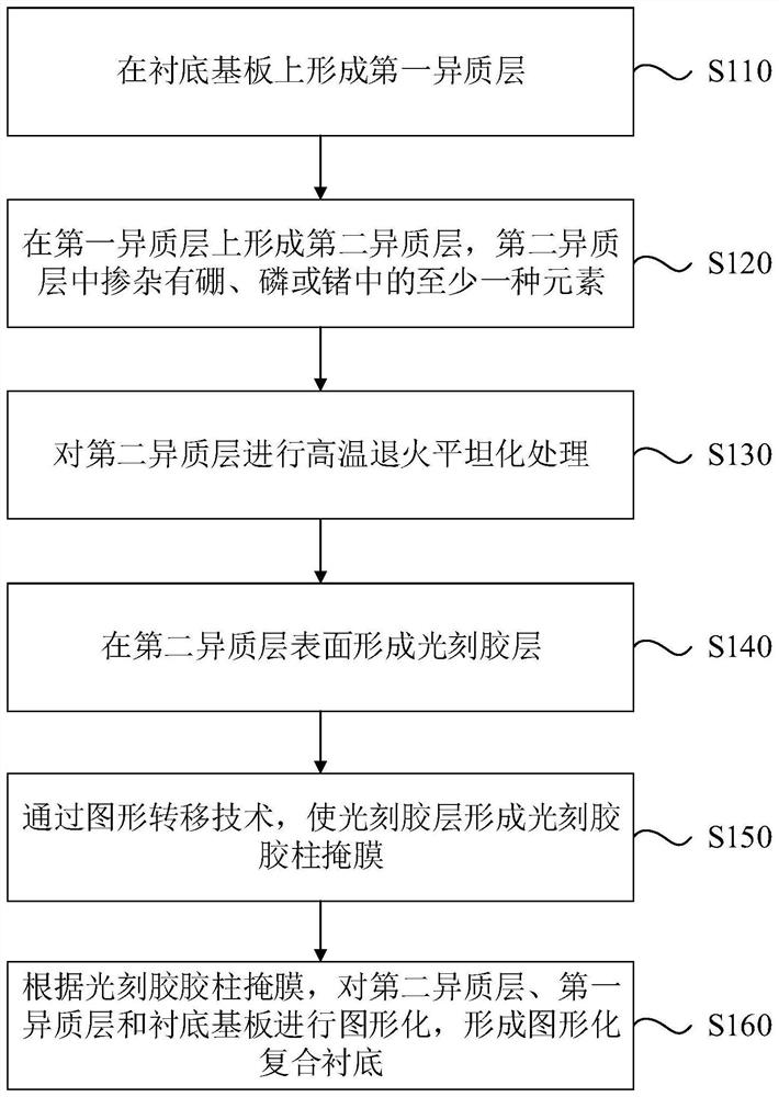
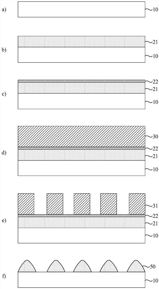
[0031] figure 1 It is a flowchart of a method for preparing a patterned composite substrate provided by an embodiment of the present invention, figure 2 yes figure 1 The structural flow diagram of the preparation method of the shown patterned composite substrate, refer to figure 1 and figure 2 , the preparation method of the patterned composite substrate comprises:

[0032] S110, forming a first heterogeneous layer on the base substrate;

[0033] refer to figure 2 In figure a), the base substrate 10 is a ...


PUM

PropertyMeasurementUnit
thicknessaaaaaaaaaa

Abstract

The embodiment of the invention discloses a patterned composite substrate, a preparation method and an LED epitaxial wafer. The preparation method of the patterned composite substrate comprises the following steps: forming a first heterogeneous layer on a substrate; forming a second heterogeneous layer on the first heterogeneous layer, wherein the second heterogeneous layer is doped with at least one element of boron, phosphorus or germanium; carrying out high-temperature annealing planarization processing on the second heterogeneous layer; forming a photoresist layer on the surface of the second heterogeneous layer; forming a photoresist column mask on the photoresist layer through a pattern transfer technology; and patterning the second heterogeneous layer, the first heterogeneous layer and the substrate according to the photoresist column mask to form a patterned composite substrate. According to the embodiment of the invention, the problems of low surface flatness and poor roughness of the existing heterogeneous layer are solved, the patterned composite substrate meeting the standard can be prepared, the growth quality of the epitaxial layer can be improved, meanwhile, the patterned composite substrate is ensured to improve the light path, and the light emitting efficiency of the LED chip is improved.

Description

technical field [0001] The embodiments of the present invention relate to the technical field of semiconductor manufacturing, and in particular to a patterned composite substrate, a preparation method and an LED epitaxial wafer. Background technique [0002] Composite patterned substrates (such as SiO 2 / Al 2 o 3 ) can further improve the crystal quality and light extraction efficiency of GaN-based LED devices. In the first aspect, SiO 2 / Al 2 o 3 Composite patterned substrates, due to SiO 2 The material itself is not suitable for GaN to grow on it, so it can promote the bending of dislocations along the side of the figure and the closing of the top of the figure, improving the crystal quality of GaN materials; the second aspect, SiO 2 / Al 2 o 3 SiO in Composite Patterned Substrates 2 The material has a larger refractive index difference with GaN, and the total reflection angle formed with the GaN material is larger, which can improve the light extraction efficienc...

Claims


Application Information

Patent Timeline
Patent Type & Authority Applications(China)
IPC IPC(8): H01L33/22H01L33/00G03F1/76
CPCH01L33/22H01L33/0075H01L33/0066G03F1/76
Inventor 谢鹏程张剑桥陆前军康凯肖桂明
Owner 广东中图半导体科技股份有限公司
Why Eureka
Try Eureka