Novel integrated DC-DC module and manufacturing method thereof
A DC-DC, module technology, applied in the direction of transformer/inductor coil/winding/connection, electrical components, transformer/inductor components, etc., can solve the problem of weak battery life, large board area and applicability problems such as poor performance, to achieve the advantages of high integration and small size, and the effect of increased battery life
- Summary
- Abstract
- Description
- Claims
- Application Information
AI Technical Summary
Problems solved by technology
Method used
Image


Examples
Embodiment 1
[0036] Embodiment 1: NR wire-wound power inductor + DC-DC conversion chip.
[0037] S1, according to Figure 4 The NR power inductor is designed with a 2.5*2.0*1.0mm nickel-zinc ferrite core. There are grooves at the bottom of the magnetic core electrode, and the metallization pattern on the electrode surface is designed according to the requirements of chip pins and winding welding requirements.
[0038] S2. Using the winding method, the wire is wound on the NR252010 magnetic core, and the lead wire is electrically connected to the magnetic core through side thermocompression welding;
[0039] S3, the semi-finished product obtained in S2 is coated with magnetic glue and cured to obtain the finished product of NR winding power inductor;
[0040] S4. Spray solder paste or implant BGA balls at the bottom pit of the NR winding power inductor corresponding to the metallization layer, then implant the DC-DC conversion chip into the bottom pit of the NR winding power inductor, and...
Embodiment 2
[0042] Embodiment 2: Laminated power inductor + DC-DC conversion chip.
[0043] S1, according to Image 6 with Figure 7 Design the internal electrode structure and external electrode structure of the 2.5*2.0*0.8mm laminated power inductor. The soft magnetic material is ferrite soft magnetic material.
[0044] S2. Carry out the production of the laminated power inductor according to the structural design of S1;
[0045] S3. Spray solder paste or implant BGA balls on the top surface of the stacked power inductor corresponding to the solder joint, and then paste the DC-DC conversion chip on the top surface of the stacked power inductor, and perform electrical connection through the reflow soldering process; or DC -The DC conversion chip is pasted on the top surface of the laminated power inductor, and then connected by bonding;
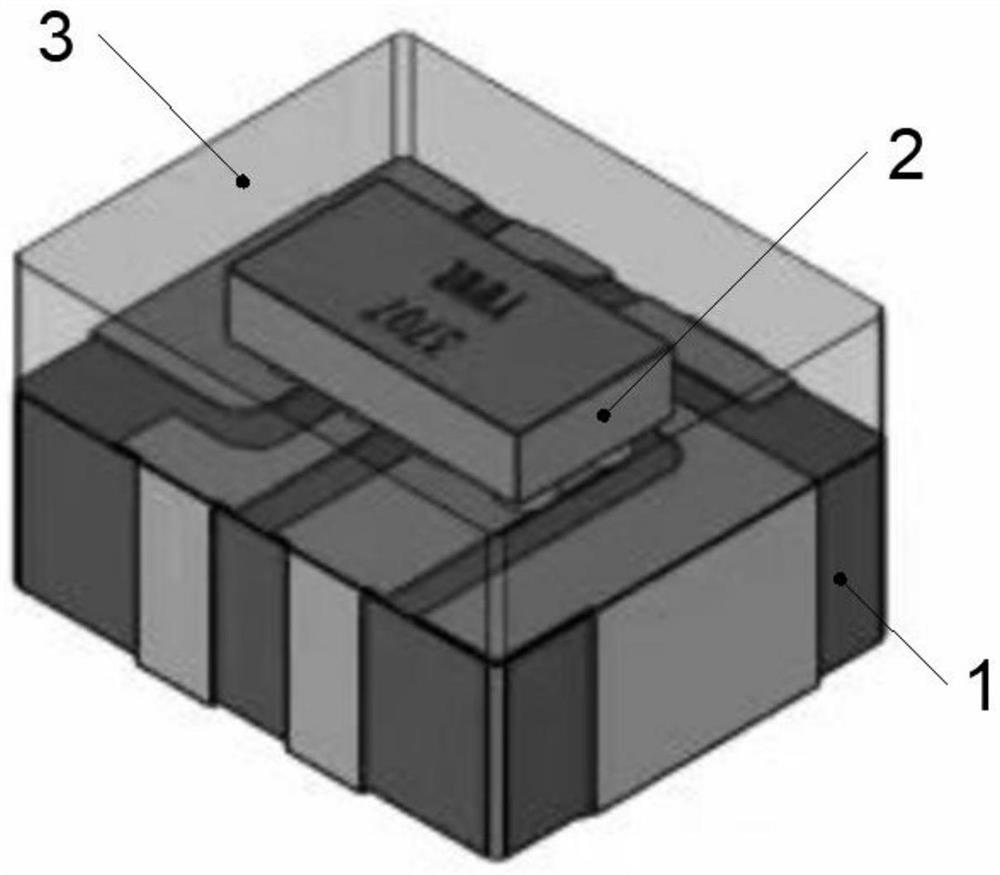
[0046] S4. Dispensing glue on the surface of the semi-finished chip obtained in S3 to protect the chip, and at the same time facilitate the absorpt...
Embodiment 3
[0047] Embodiment 3: Integral molding power inductor + DC-DC conversion chip.
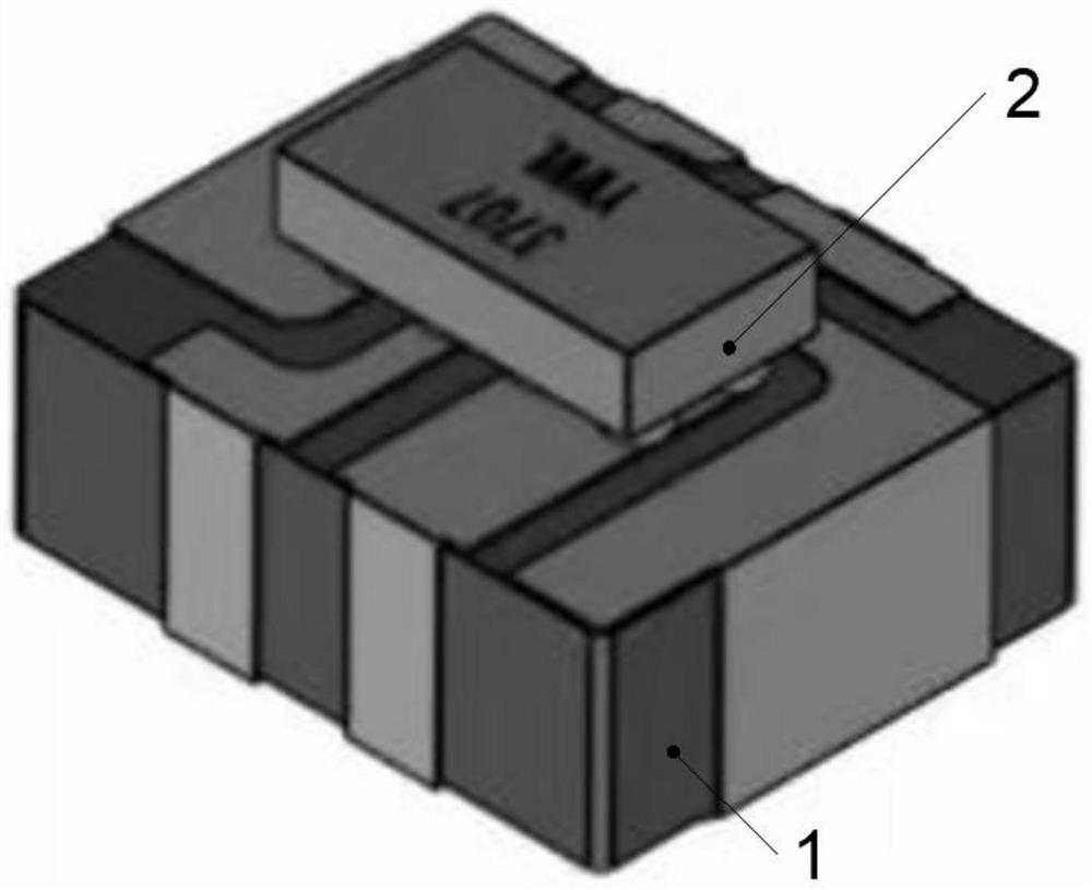
[0048] S1, according to figure 1 Carry out 2.5*2.0*0.8mm for the production of integral molding inductors, and lead wires are drawn on the side of the product at 2.0*0.8mm.
[0049] S2. Carry out full insulation coating on the integrally formed power inductor product obtained in S1;
[0050] S3. Grind the 2.0*0.8mm side of the integrally formed power inductor to expose the leads; etch a pre-designed pattern on the other surface of the integrally formed power inductor by laser etching, such as figure 1 shown;
[0051] S4. Perform electroplating on the semi-finished product obtained in S3 to obtain the required external electrodes and electrical circuits.
[0052] S5. Spray solder paste or implant BGA balls on the top surface of the integrally formed power inductor obtained in S4, then paste the DC-DC conversion chip on the top surface of the laminated power inductor, and perform electrical connec...
PUM
 Abstract
Description
Claims
Application Information
 - R&D
- Intellectual Property
- Life Sciences
- Materials
- Tech Scout
- Unparalleled Data Quality
- Higher Quality Content
- 60% Fewer Hallucinations
Browse by: Latest US Patents, China's latest patents, Technical Efficacy Thesaurus, Application Domain, Technology Topic, Popular Technical Reports.
© 2025 PatSnap. All rights reserved.Legal|Privacy policy|Modern Slavery Act Transparency Statement|Sitemap|About US| Contact US: help@patsnap.com