Silicon carbide MOSFET device integrated with SBD and preparation method thereof

A silicon carbide and device technology, applied in the field of silicon carbide MOSFET devices and their preparation, can solve the problems of high turn-on voltage drop and reverse recovery loss, unfavorable to the reliability of silicon carbide devices, increased reverse bias leakage current, etc. , to increase reliability, reduce impact, and improve power density

Pending Publication Date: 2022-03-22
ZHUZHOU CRRC TIMES SEMICON CO LTD
View PDF0 Cites 4 Cited by
  • Summary
  • Abstract
  • Description
  • Claims
  • Application Information

AI Technical Summary

Problems solved by technology

However, since the body diode is a PIN structure device, it will generate high turn-on voltage drop and reverse recovery loss
At the same time, the conduction of SiC bipolar devices will induce electron-hole recombination, which will expand the stacked layers in the body, increase the device voltage drop, and increase the reverse bias leakage current, which is not conducive to the reliability of silicon carbide devices.

Method used


Image

  • Silicon carbide MOSFET device integrated with SBD and preparation method thereof
  • Silicon carbide MOSFET device integrated with SBD and preparation method thereof
  • Silicon carbide MOSFET device integrated with SBD and preparation method thereof

Examples


Embodiment Construction

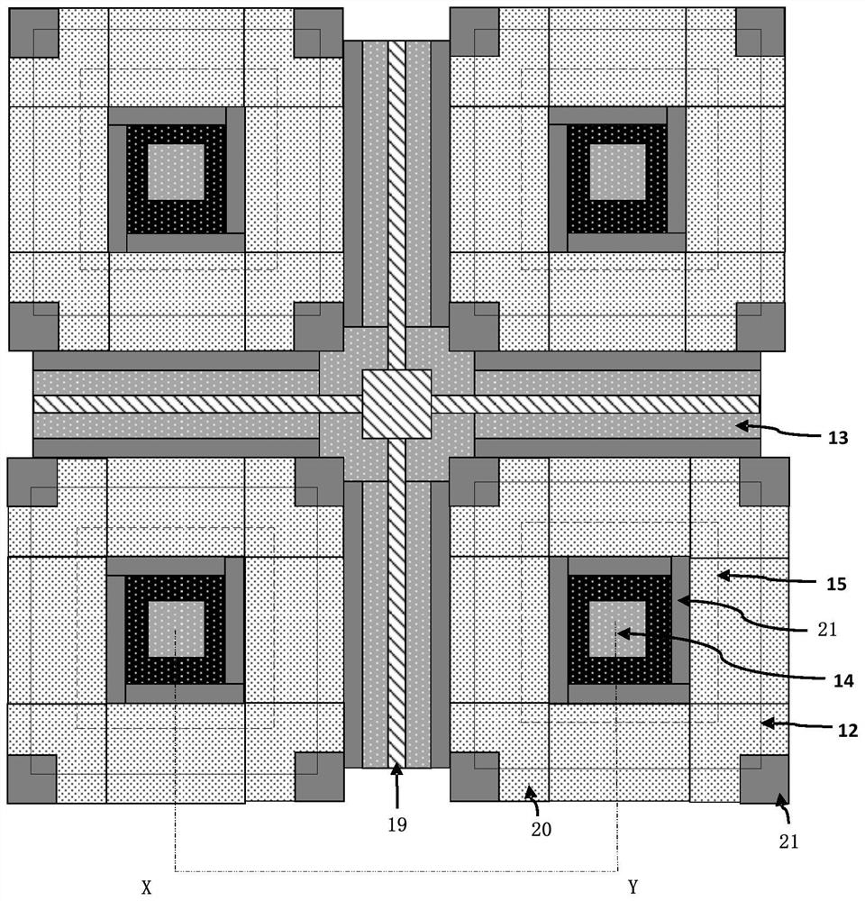
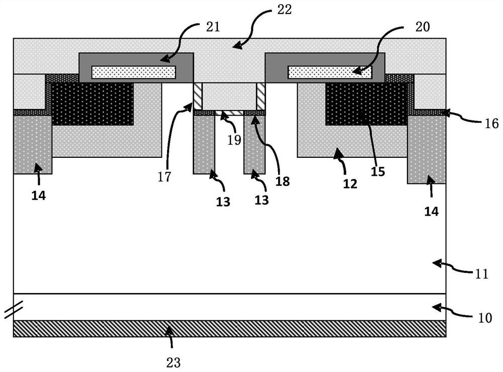
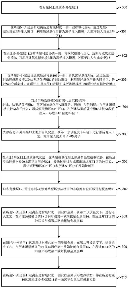
[0052] The implementation of the present invention will be described in detail below in conjunction with the accompanying drawings and examples, so as to fully understand and implement the process of how to apply technical means to solve technical problems and achieve technical effects in the present invention. It should be noted that, as long as there is no conflict, each embodiment and each feature in each embodiment of the present invention can be combined with each other, and the formed technical solutions are all within the protection scope of the present invention.

[0053] figure 1 It is a top view of the silicon carbide MOSFET device integrating SBD of the present invention, figure 2 for figure 1 Cross-sectional view in the X-Y direction. Such as Figure 1-Figure 2 As shown, the SBD-integrated silicon carbide MOSFET device of this embodiment may include several cell structures. The cellular structure includes a substrate 10, an N-epitaxial layer 11 formed on the s...


PUM

PropertyMeasurementUnit
depthaaaaaaaaaa
depthaaaaaaaaaa
depthaaaaaaaaaa

Abstract

The invention discloses a silicon carbide MOSFET device integrated with an SBD and a preparation method of the silicon carbide MOSFET device. The silicon carbide MOSFET device comprises a substrate, an N-epitaxial layer, a P well region, a P + region of a junction field effect region, a P + region and an N + region of a source groove region, a first ohmic contact metal layer, a first Schottky contact metal layer, a second ohmic contact metal layer and a second Schottky contact metal layer. The P + region of the junction field effect region is positioned on one side, far away from the N + region, of the P well region; the second ohmic contact metal layer covers one surface, deviating from the N-epitaxial layer, of the P + region of the junction field effect region; the first Schottky contact metal layer is located on the side, away from the P well region, of the second ohmic contact metal layer. And the second Schottky contact metal layer is arranged on one side, deviating from the P + region of the junction field effect region, of the second ohmic contact metal layer, and is parallel to the P + region of the junction field effect region. The source contact resistance can be reduced, the through-current capability of the silicon carbide device is improved, and the reliability of the silicon carbide device is improved.

Description

technical field [0001] The invention belongs to the technical field of semiconductors, and in particular relates to an SBD-integrated silicon carbide MOSFET device and a preparation method thereof. Background technique [0002] Silicon carbide metal oxide semiconductor field effect transistor (SiC MOSFET) has the characteristics of low on-resistance, fast switching speed, high temperature resistance, etc., and has great application advantages in high-voltage frequency conversion, new energy vehicles, rail transit and other fields. In order to improve the current capacity of SiC MOSFET, the size of the cell is often compressed to increase the flow area and improve the flow capacity. When the cell size is continuously compressed, the contact area of ​​the source hole is also reduced, and the source contact resistance will become very large, which is not conducive to the reduction of the overall resistance of the device. [0003] At the same time, in application scenarios such...

Claims


Application Information

Patent Timeline
Patent Type & Authority Applications(China)
IPC IPC(8): H01L29/06H01L29/08H01L29/78H01L29/872H01L27/07H01L21/82H01L21/336H01L21/329
CPCH01L29/7827H01L29/66068H01L27/0727H01L21/8213H01L29/872H01L29/6606H01L29/0684H01L29/0696H01L29/0847
Inventor 罗烨辉王亚飞郑昌伟王志成刘启军刘小东李诚瞻
Owner ZHUZHOU CRRC TIMES SEMICON CO LTD
Why Eureka
Try Eureka