Preparation process of gold finger gold plating and chemical gold copper-based circuit board

A preparation process and gold finger technology, which is applied to circuit substrate materials, printed circuit components, etc., can solve problems such as limited lateral cutting force and axial force, increased difficulty in manufacturing and processing, and weak chip removal ability, so as to improve process capability , The effect of improving the quality of solder resist printing and reducing the cost

Active Publication Date: 2022-03-25
BOLUO KONKA EXACTITUDE SCI TECH
View PDF9 Cites 0 Cited by
  • Summary
  • Abstract
  • Description
  • Claims
  • Application Information

AI Technical Summary

Problems solved by technology

[0006] 1. Difficulty in pure copper small hole drilling technology: especially when the drilling tool diameter is less than 0.7mm, the lateral cutting force and axial force it can withstand are very limited, and the ability to shed chips is very weak, which is a challenge for drilling Very big;
[0007] 2. Small hole copper plating technology on metal substrate: it is prone to the problems of hole breakage, crack and pull-off;
[0009] 4. Difficulties in the surface treatment technology of electro-nickel gold plus chemical gold: two different surface treatments of gold plating and soft gold are performed on the same board at the same time. The two processes and procedures are different, which increases the difficulty of manufacturing and processing;
[0010] 5. Difficulties in forming and processing metal copper substrates: traditional thick copper plate shape processing generally uses mechanical drilling machines for forming processing, and there are some technical shortcomings;

Method used


Image

  • Preparation process of gold finger gold plating and chemical gold copper-based circuit board
  • Preparation process of gold finger gold plating and chemical gold copper-based circuit board
  • Preparation process of gold finger gold plating and chemical gold copper-based circuit board

Examples


Embodiment Construction

[0064] The following will clearly and completely describe the technical solutions in the embodiments of the present invention with reference to the accompanying drawings in the embodiments of the present invention. Obviously, the described embodiments are only some, not all, embodiments of the present invention. The specific embodiments described here are only used to explain the present invention, not to limit the present invention. Based on the embodiments of the present invention, all other embodiments obtained by persons of ordinary skill in the art without making creative efforts belong to the protection scope of the present invention.

[0065] The present invention provides the embodiment shown in the accompanying drawings:

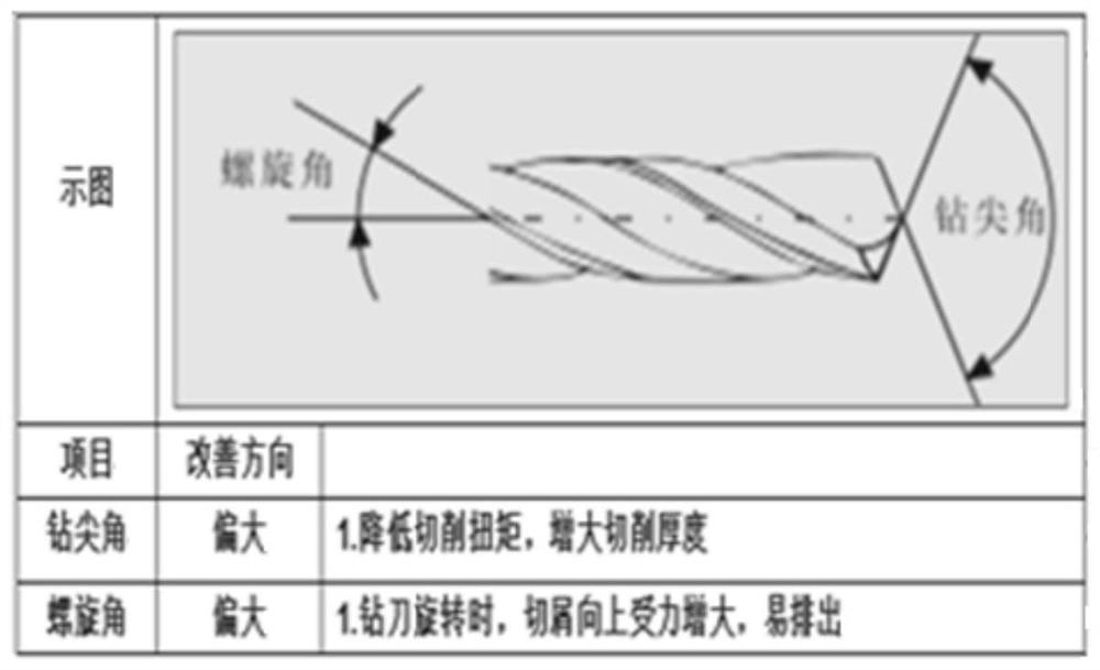
[0066] 1. Analysis of the difficulty of drilling small holes on metal copper substrates: Due to the high demand for heat dissipation or plate making of the instrument test board, the material used for the copper substrate is red copper with high cop...


PUM


Abstract

The invention discloses a preparation process of a gold finger gold plating and chemical gold copper-based circuit board. Comprising a solution to the problem that a drilling tool is easy to wear / break, a solution to the technical difficulty of electroplating and hole plating of a copper substrate, a solution to the technical difficulty of solder mask printing of a thick copper plate, a solution to the technical difficulty of surface treatment nickel gold electroplating and chemical gold plating, and a solution to the technical difficulty of molding processing of a metal copper substrate. According to the invention, through the overall process design of the preparation of the gold finger gold plating and chemical gold copper-based circuit board, the cutter and parameter selection for processing the small hole of the copper substrate are optimized; a chemical copper deposition autocatalytic reaction is induced through activation of the palladium core, and after treatment in the step, a layer of chemical copper can be deposited on the surface or the hole wall of the metal copper substrate to be precisely combined with the surface and the hole wall of the metal copper substrate; through flow optimization, the solder resist printing quality of the thick copper plate is improved; as the integration level of the IC is higher and higher, the IC pins are more and denser; the laser has high applicability and sensitivity, and the influence range of cutting is reduced.

Description

technical field [0001] The invention belongs to the technical field of gold-finger gold-added gold-copper base circuit board preparation technology, and in particular relates to a preparation process of gold-finger gold-added gold-copper base circuit board. Background technique [0002] Copper substrate is the most expensive kind of metal substrate, and its thermal conductivity is many times better than that of aluminum substrate and iron substrate. It is suitable for high-frequency circuits and areas with large changes in high and low temperature, as well as heat dissipation of precision communication equipment and architectural decoration industries. The circuit board made of copper substrate has the advantages of good thermal conductivity, electrical insulation performance and mechanical processing performance. The substrate material is generally copper plate, which can provide better thermal conductivity, and its heat dissipation effect is also better than that of aluminu...

Claims


Application Information

Patent Timeline
Patent Type & Authority Applications(China)
IPC IPC(8): B23P15/00H05K1/05
CPCB23P15/00H05K1/05
Inventor 雷仁庆尹国强钟晓环刘建波
Owner BOLUO KONKA EXACTITUDE SCI TECH
Why Eureka
Try Eureka