
Preparation process and structure of MTM type anti-fuse unit based on ONO medium

A preparation process and anti-fuse technology, applied in electrical components, semiconductor/solid-state device manufacturing, electrical solid-state devices, etc., can solve the problems of high programming power consumption, small memory capacity, large chip area, etc., to reduce programming current, Strong operability, the effect of reducing static power consumption

Pending Publication Date: 2022-04-05
58TH RES INST OF CETC
View PDF0 Cites 0 Cited by
  • Summary
  • Abstract
  • Description
  • Claims
  • Application Information

AI Technical Summary

Problems solved by technology

[0005] The purpose of the present invention is to provide a preparation process and structure of an MTM antifuse unit based on an ONO medium, so as to solve the problems of small capacity, large chip area, and high programming power consumption of traditional MTM antifuse memory

Method used


Image

  • Preparation process and structure of MTM type anti-fuse unit based on ONO medium
  • Preparation process and structure of MTM type anti-fuse unit based on ONO medium
  • Preparation process and structure of MTM type anti-fuse unit based on ONO medium

Examples


Embodiment Construction

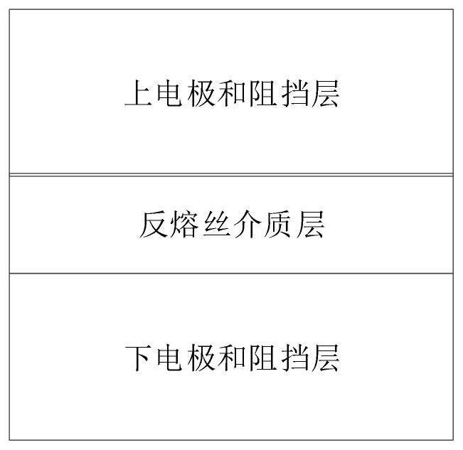
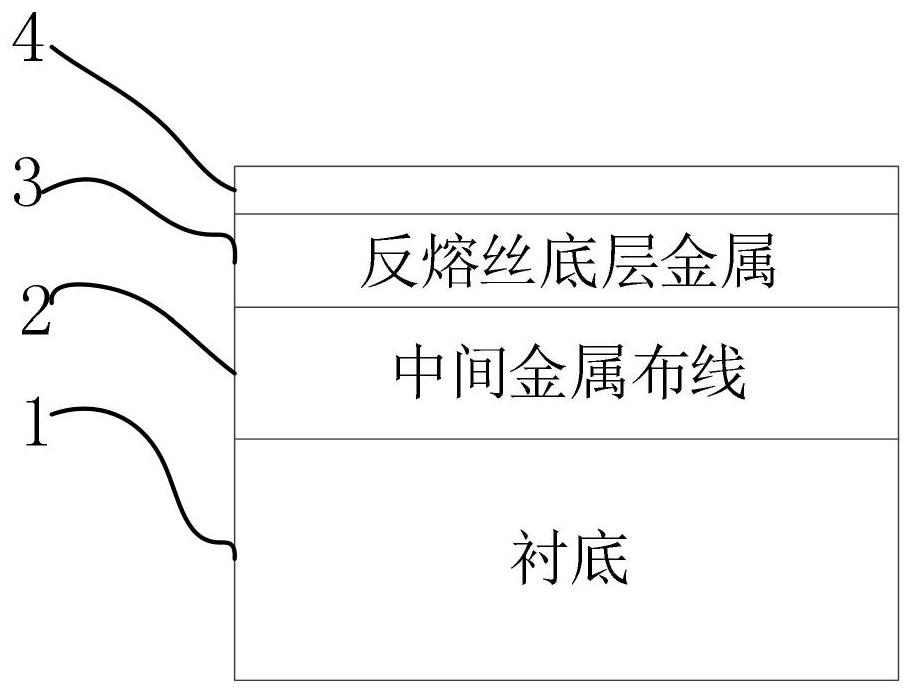
[0041] The preparation process and structure of an ONO medium-based MTM antifuse unit proposed by the present invention will be further described in detail below in conjunction with the accompanying drawings and specific embodiments. Advantages and features of the present invention will be apparent from the following description and claims. It should be noted that all the drawings are in a very simplified form and use imprecise scales, and are only used to facilitate and clearly assist the purpose of illustrating the embodiments of the present invention.

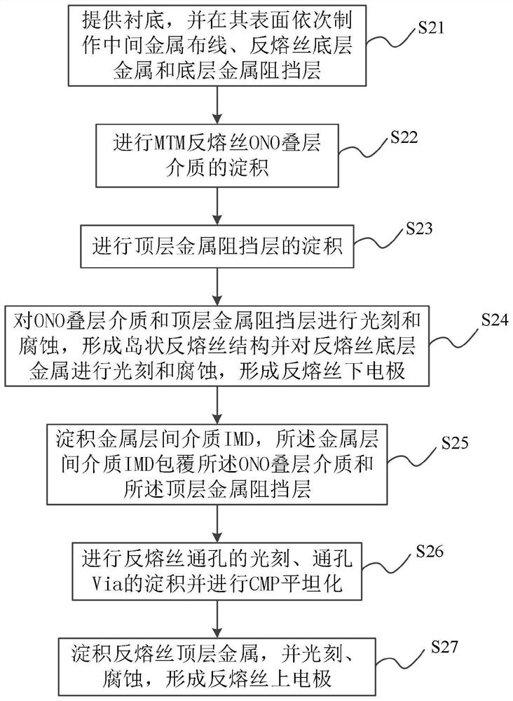
[0042] The invention provides a preparation process of an MTM type antifuse unit based on an ONO medium, the process of which is as follows figure 2 shown, including the following steps:

[0043] Step S21, providing a substrate, and sequentially fabricating MOS device levels and intermediate metal wiring, antifuse bottom metal and bottom metal barrier layer on its surface;

[0044] Step S22, depositing the MTM antifuse ON...


PUM

PropertyMeasurementUnit
Thicknessaaaaaaaaaa
Thicknessaaaaaaaaaa
Thicknessaaaaaaaaaa

Abstract

The invention discloses a preparation process and structure of an ONO medium-based MTM type anti-fuse unit, and belongs to the field of microelectronic process manufacturing. Providing a substrate, and sequentially manufacturing an intermediate metal wiring, an anti-fuse bottom metal and a bottom metal barrier layer on the surface of the substrate; carrying out the deposition of an MTM anti-fuse ONO laminated medium; depositing a top metal barrier layer; photoetching and corroding the ONO laminated medium and the top metal barrier layer to form an island-shaped anti-fuse structure; depositing a metal interlayer dielectric (IMD), wherein the metal interlayer dielectric (IMD) coats the ONO laminated dielectric and the top metal barrier layer; photoetching of an anti-fuse through hole and deposition of a through hole Via are carried out, and CMP planarization is carried out; and depositing anti-fuse top layer metal, and performing photoetching and corrosion to form an anti-fuse upper electrode. The novel MTM anti-fuse medium technology is adopted, the programming current of the anti-fuse unit is remarkably reduced, the layout area of the anti-fuse storage unit Bitcell is reduced, and the integration level of the anti-fuse storage unit is improved by more than 10 times.

Description

technical field [0001] The invention relates to the technical field of microelectronics process manufacturing, in particular to a preparation process and structure of an MTM type antifuse unit based on an ONO medium. Background technique [0002] As an OTP (One Time Programming, one-time programmable) device, the MTM antifuse unit is usually used in FPGA, PROM and other circuit products. According to actual needs, the antifuse unit in the circuit is programmed to realize the logic function or storage of the circuit. Features. This type of MTM antifuse circuit has the characteristics of excellent radiation resistance, strong confidentiality, and good flexibility, and has broad application prospects in aerospace and military fields. [0003] Such as figure 1 As shown, the MTM antifuse unit structure is located between the two layers of metal wiring in the circuit, and is composed of the antifuse dielectric layer, the dielectric barrier layer on the upper and lower sides, and...

Claims


Application Information

Patent Timeline
IPC IPC(8): H01L21/8246H01L23/525H01L27/112
Inventor 王印权郑若成洪根深吴建伟贺琪胡君彪郝新焱
Owner 58TH RES INST OF CETC
Learn More