Feedback type two-end fuse storage unit and preparation method thereof
A memory unit and feedback technology, which is applied in the direction of electrical components, semiconductor/solid-state device manufacturing, semiconductor devices, etc., can solve the problems of slow programming speed and high power consumption, and achieve easy integration, reduced power consumption, and lower programming voltage Effect
- Summary
- Abstract
- Description
- Claims
- Application Information
AI Technical Summary
Problems solved by technology
Method used
Image
Examples
Embodiment 1
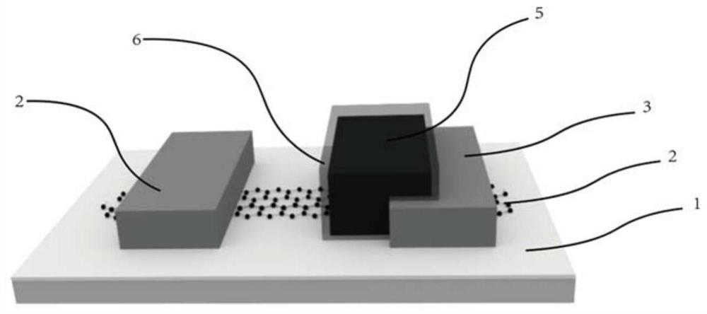
[0044] An embodiment of the present invention provides a feedback type two-terminal fuse storage unit, such as image 3 As shown, there is a substrate 1, a graphene channel 2 on the substrate 1, a drain electrode 3 and a source electrode 4 at both ends of the graphene channel 2, and a drain electrode 3 and a source electrode 4 are formed between the drain electrode 3 and the source electrode 4. The gate window has a metal gate 5 in the gate window, the metal gate 5 is perpendicular to the extension direction of the graphene channel 2 and is in electrical contact with the above-mentioned drain, an oxide layer is formed on the outer surface of the metal gate 5, and the above-mentioned metal gate There is a gate oxide layer between 5 and the above-mentioned graphene channel 2 . In this embodiment, the graphene channel 2 is a single-layer graphene material. In another embodiment, the graphene channel 2 is a graphene nanoribbon. A drain electrode 3 and a source electrode 4 are res...
Embodiment 2
[0047] This embodiment proposes a method for preparing a feedback type two-terminal fuse storage unit, which includes the following steps:
[0048]For the subsequent micro-nano processing and pattern overlay of the device, marks are first made on the substrate. Because of the strong adhesion between titanium and the substrate, 5nm titanium and 50nm gold are used to make the marks to prevent the marks from falling off.
[0049] like Figure 4 As shown, a silicon monoxide substrate 101 is provided, and a layer of graphene material is transferred on the silicon oxide substrate 101. Specifically, firstly, the graphene material is obtained by in-situ growth on the copper foil by CVD, and then the graphene material on the copper foil is grown. The graphene material is transferred to the silicon oxide substrate, and the graphene channel 102 is obtained by patterning and etching the graphene material by electron beam exposure (EBL) and oxygen plasma etching (ICP), respectively. In ot...
Embodiment 3
[0053] This embodiment proposes another method for preparing a feedback type two-terminal fuse storage unit, and the specific steps are as follows:
[0054] The graphene channel 202 , the drain electrode 203 and the source electrode 204 are formed on the substrate 201 according to the steps in Embodiment 2. then as Figure 11 As shown, the grid window is patterned by electron beam exposure, and then a metal layer Al is deposited between the drain electrode 203 and the source electrode 204 by electron beam evaporation to form a metal grid 205, and the metal grid Al and the drain electrode 203 are electrically connected. touch.
[0055] further as Figure 12 As shown, the structure formed by the above steps is annealed and oxidized at a temperature of 120°C-150°C for 30-60min, and in this embodiment, it is baked at 150°C for 40min, so that the graphene channel 202 and the metal gate 205 A dense metal oxide film is formed at the interface. Among them, the gate of the fuse mem...
PUM
 Abstract
Description
Claims
Application Information


