Packaging structure and packaging method of cascaded GaN-based power device

A technology for packaging structure and power devices, which is applied in the manufacturing of semiconductor devices, electric solid state devices, semiconductor/solid state devices, etc., to reduce parasitic inductance, improve switching performance and energy efficiency, and improve heat dissipation performance and reliability.

Pending Publication Date: 2022-04-05
珠海镓未来科技有限公司
View PDF0 Cites 5 Cited by
  • Summary
  • Abstract
  • Description
  • Claims
  • Application Information

AI Technical Summary

Problems solved by technology

[0005] The invention provides a packaging structure and packaging method of a cascaded GaN-based power device to solve the problems of heat dissipation and parasitic inductance caused by the chip being installed in the cascaded power device, and improve the performance of the hybrid device

Method used


Image

  • Packaging structure and packaging method of cascaded GaN-based power device
  • Packaging structure and packaging method of cascaded GaN-based power device
  • Packaging structure and packaging method of cascaded GaN-based power device

Examples


Embodiment Construction

[0050] The present invention will be further described in detail below in conjunction with the accompanying drawings and embodiments. It should be understood that the specific embodiments described here are only used to explain the present invention, but not to limit the present invention. In addition, it should be noted that, for the convenience of description, only some structures related to the present invention are shown in the drawings but not all structures.

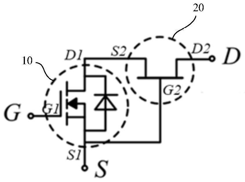
[0051] figure 1 It is a schematic diagram of a cascaded mixing tube device provided by the embodiment of the present invention, refer to figure 1 , the cascaded hybrid tube device has a forward turn-on voltage enhanced mode of operation through cascading, wherein the low-voltage Si-based MOSFET chip 10 controls the on and off of the entire device, and the high-voltage depletion-type GaN-based HEMT chip 20 is in the device Play the role of withstand high voltage when shut down.

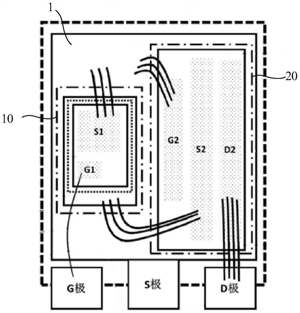
[0052] figure 2 yes figure 1 A...


PUM

PropertyMeasurementUnit
thicknessaaaaaaaaaa
thicknessaaaaaaaaaa
diameteraaaaaaaaaa

Abstract

The embodiment of the invention discloses a packaging structure and a packaging method of a cascaded GaN-based power device. According to the packaging structure, an HEMT chip, an MOSFET chip, a frame base island and a conductive connection structure are packaged in a plastic packaging material; the first side surface of the frame base island is provided with a groove, and the conductive connection structure is fixed in the groove and is insulated from the frame base island. The MOSFET chip is inversely arranged on the first side surface of the frame base island, a grid electrode of the MOSFET chip is electrically connected with the conductive connection structure, and a source electrode of the MOSFET chip is electrically connected with a non-groove area of the first side surface; the HEMT chip is arranged on the first side surface of the frame base island, and the source electrode of the HEMT chip is electrically connected with the drain electrode of the MOSFET chip through a lead. The grid electrode is electrically connected with the frame base island through a lead. According to the embodiment of the invention, the heat dissipation performance and reliability of the chip are improved, meanwhile, the parasitic inductive reactance is reduced, and the switching performance and the energy efficiency are improved.

Description

technical field [0001] Embodiments of the present invention relate to the field of semiconductor technology, and in particular to a packaging structure and a packaging method of a cascaded GaN-based power device. Background technique [0002] Gallium nitride (GaN) power devices can meet the application requirements of high temperature, high voltage and high frequency due to their advantages such as large band gap, high saturation electron mobility and high thermal conductivity. Fields such as power radar, electronic countermeasures and satellite communication have been more and more widely used. [0003] At present, the most widely used and most mature is the GaN material-based high electron mobility transistor (High Electron Mobility Transistor, HEMT). GaN-based HEMTs can be divided into enhancement mode and depletion mode. Among them, the enhanced high-voltage GaN-based HEMT manufacturing process is still immature. For example, the threshold voltage is small, and the dri...

Claims


Application Information

Patent Timeline
Patent Type & Authority Applications(China)
IPC IPC(8): H01L23/495H01L25/18H01L21/48H01L21/60
CPCH01L2224/48137H01L2224/48257H01L2224/49111H01L2224/78H01L2224/18H01L2224/48091H01L2224/48247H01L2224/85181H01L2924/181H01L2224/0603H01L2924/00014H01L2924/00012
Inventor 吴毅锋王美玉曾凡明李生东
Owner 珠海镓未来科技有限公司
Why Eureka
Try Eureka