Hot carrier injection type single-pixel photoelectric detection device, preparation method and system

A photodetector and hot carrier technology, applied in the field of photodetection, can solve the problem of unsatisfactory photoelectric response speed of photodetector devices, and achieve the effects of avoiding the adsorption of impurities at the interface, avoiding damage, and avoiding pollution

Pending Publication Date: 2022-04-08
HUAZHONG UNIV OF SCI & TECH
View PDF0 Cites 0 Cited by
  • Summary
  • Abstract
  • Description
  • Claims
  • Application Information

AI Technical Summary

Problems solved by technology

[0005] In view of the above defects or improvement needs of the prior art, the present invention provides a hot carrier injection type single-pixel photodetection device, a preparation method and a system, the purpose of which is to optimize the contact area between the interface metal and the semiconductor, and the cleanliness of the interface Improve the transmission speed, thereby solving the technical problem of unsatisfactory photoelectric response speed of the photodetector device

Method used


Image

  • Hot carrier injection type single-pixel photoelectric detection device, preparation method and system
  • Hot carrier injection type single-pixel photoelectric detection device, preparation method and system
  • Hot carrier injection type single-pixel photoelectric detection device, preparation method and system

Examples


Embodiment 1

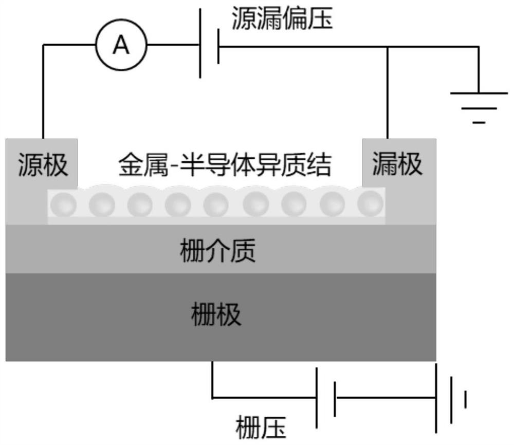
[0036] Cr / Au / Au-MoS 2 / Au / Cr lateral devices, see figure 1 .

[0037] (1) First in the clean Si / SiO 2 3nm Au is deposited on the surface of the substrate, and the rapid heating and cooling annealing process is realized by a moving slide tube furnace, and Si / SiO with 3nm Au is deposited 2The substrate is annealed at 550° C. for 7 minutes to form uniformly distributed nanoparticles with a particle size of 20-40 nm.

[0038] (2) Subsequent preparation of Au-MoS on the surface of Au nanoparticles by chemical vapor deposition 2 Heterojunction, choose sulfur powder and molybdenum oxide as the reaction source, set the temperature in the central temperature zone of the single temperature zone tube furnace used for the reaction to 625-750°C, and the reaction time is 3-10min. After natural cooling, uniform and continuous patterns can be obtained. oxidized heterojunction samples.

[0039] (3) Si with a thickness of 2mm is used as the gate electrode, and SiO with a thickness of 300nm...

Embodiment 2

[0046] Cr / Au / Ag-WSe 2 / Au / Cr lateral devices: first on clean Si / SiO 2 5nm Ag is deposited on the surface of the substrate, and annealed at 350°C for 7min to form evenly distributed nanoparticles with a particle size of 20-40nm. Subsequently, Ag-WSe was prepared on the surface of Ag nanoparticles by chemical vapor deposition. 2 For heterojunction, tin powder and tungsten oxide are selected as the reaction source. With 2mm thick Si as the gate electrode, 300nm thick SiO 2 As the gate dielectric, expose the electrode area on the surface of the sample and deposit Cr / Au electrodes as source and drain electrodes to form a lateral device. A bias voltage of 0-10V is applied to the source and drain electrodes, and a rapid photoelectric response is obtained when light is applied with a wavelength range of 365-800nm, and the channel performance can be adjusted by applying a voltage of 0-60V to the gate. The device is placed in a single-pixel imaging system, and a light source with a ...

Embodiment 3

[0048] Cr / Au / Au-CsPbBr 3 / Au / Cr Lateral Devices: Preparation of Au-CsPbBr 3 heterojunction, first in clean Si / SiO 2 3nm Au is deposited on the surface of the substrate, and the rapid heating and cooling annealing process is realized by a moving slide tube furnace, and Si / SiO with 3nm Au is deposited 2 The substrate is annealed at 550° C. for 7 minutes to form uniformly distributed nanoparticles with a particle size of 20-40 nm. Preparation of Au-CsPbBr by Chemical Vapor Deposition 3 Sample, with Si as the gate electrode, SiO 2 As the gate dielectric, Cr / Au electrodes are deposited on the surface of the sample as source and drain electrodes to form a lateral device. A fast photoelectric response is obtained when the source and drain electrodes are applied with proper bias voltage and light, and the channel performance can be adjusted by applying a voltage on the gate. The device is placed in a single-pixel imaging system, and a light source with a certain wavelength is use...


PUM

PropertyMeasurementUnit
particle diameteraaaaaaaaaa
thicknessaaaaaaaaaa
thicknessaaaaaaaaaa

Abstract

The invention discloses a hot carrier injection type single-pixel photoelectric detection device, a preparation method and a system. The method comprises the following steps: depositing metal on the surface of a substrate, and annealing to form metal nanoparticles; forming a two-dimensional semiconductor layer on the surfaces of the metal nanoparticles by adopting a chemical vapor deposition method, and forming a steep metal-semiconductor Schottky heterojunction with a clean interface; and preparing a grid electrode, a grid dielectric layer, a source electrode and a drain electrode on the semiconductor layer to obtain the hot carrier injection type single-pixel photoelectric detector. A metal-semiconductor Schottky heterojunction with a clean interface is formed, local surface plasmons of metal nanoparticles are subjected to non-radiative attenuation to generate hot carriers under illumination, and the hot carriers pass through a Schottky barrier between metal and a semiconductor to be injected into the semiconductor, so that the metal-semiconductor Schottky heterojunction with the clean interface is formed. Picosecond-level ultrafast transmission of hot carriers and ultrafast response to incident light are realized; and single-pixel photoelectric imaging with ultra-high response speed, wide spectrum and low cost can be realized.

Description

technical field [0001] The invention belongs to the technical field of photoelectric detection, and more specifically relates to a hot carrier injection type single-pixel photodetection device, a preparation method and a system. Background technique [0002] Photoelectric imaging technology is an effective extension of human eye observation, and it is also an important cornerstone of research and development in military, medical, industrial development and other fields. Ultrafast imaging technology is an effective means to effectively observe ultrafast phenomena or ultrafast processes, and is an important part of the development of optoelectronic information in the future. [0003] CCD and CMOS cameras are array structure imaging cameras widely used in industrial production and daily life, and their basic principles are to convert light signals into charge signals. Among them, CMOS has a large production scale, fast production speed, and low cost. The disadvantage is that i...

Claims


Application Information

Patent Timeline
Patent Type & Authority Applications(China)
IPC IPC(8): H01L31/18B82Y20/00B82Y40/00C23C16/30C23C16/44H01L31/108
CPCY02P70/50
Inventor 李渊刘然刘盛洪李少华翟天佑
Owner HUAZHONG UNIV OF SCI & TECH
Why Eureka
Try Eureka