Gallium arsenide solar cell with gradient tunnel junction and manufacturing method of gallium arsenide solar cell
A technology for solar cells and manufacturing methods, which is applied to circuits, photovoltaic power generation, electrical components, etc., can solve the problems of reducing the current density of solar cells, reducing the crystal quality of top cells, and narrowing the production process window, so as to reduce light absorption capacity and improve tunneling. Penetration ability, the effect of improving crystal quality
- Summary
- Abstract
- Description
- Claims
- Application Information
AI Technical Summary
Problems solved by technology
Method used
Image
Examples
Embodiment 1
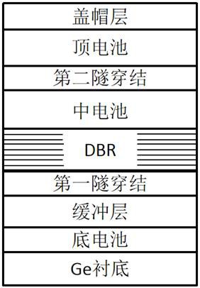
[0047] A gallium arsenide solar cell with a graded tunnel junction, from bottom to top is Ge substrate, bottom cell, buffer layer, first tunnel junction, DBR, middle cell, second tunnel junction, top cell and A capping layer; wherein, the first tunnel junction and the second tunnel junction have the same structure, and both adopt a graded tunnel junction structure.
[0048] The specific manufacturing method of the gallium arsenide solar cell is as follows:
[0049] S1. On a P-type Ge substrate, pass PH at high temperature 3 In the form of diffusion, the emitter region of the bottom cell is formed, and then the GaInP nucleation layer is grown, and the nucleation layer serves as the window layer of the bottom cell at the same time;
[0050] S2. Then grow In on the bottom cell 0.01 GaAs buffer layer, where In 0.01 GaAs buffer layer thickness is 0.1μm;
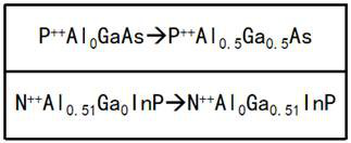
[0051] S3. Then grow a first tunnel junction on the buffer layer, the first tunnel junction is N ++ Al x1 Ga y1 InP / P ++...
Embodiment 2
[0058] A gallium arsenide solar cell with a graded tunnel junction, from bottom to top is Ge substrate, bottom cell, buffer layer, first tunnel junction, DBR, middle cell, second tunnel junction, top cell and A capping layer; wherein, the first tunnel junction and the second tunnel junction have the same structure, and both adopt a graded tunnel junction structure.
[0059] The specific manufacturing method of the gallium arsenide solar cell is as follows:
[0060] S1. On a P-type Ge substrate, pass PH at high temperature 3 In the form of diffusion, the emitter region of the bottom cell is formed, and then the GaInP nucleation layer is grown, and the nucleation layer serves as the window layer of the bottom cell at the same time;
[0061] S2. Then grow In on the bottom cell 0.01 GaAs buffer layer, where In 0.01 GaAs buffer layer thickness is 0.5μm;
[0062] S3. Then grow a first tunnel junction on the buffer layer, the first tunnel junction is N ++ Al x1 Ga y1 InP / P ++...
Embodiment 3
[0069] A gallium arsenide solar cell with a graded tunnel junction, from bottom to top is Ge substrate, bottom cell, buffer layer, first tunnel junction, DBR, middle cell, second tunnel junction, top cell and A capping layer; wherein, the first tunnel junction and the second tunnel junction have the same structure, and both adopt a graded tunnel junction structure.
[0070] The specific manufacturing method of the gallium arsenide solar cell is as follows:
[0071] S1. On a P-type Ge substrate, pass PH at high temperature 3 In the form of diffusion, the emitter region of the bottom cell is formed, and then the GaInP nucleation layer is grown, and the nucleation layer serves as the window layer of the bottom cell at the same time;
[0072] S2. Then grow In on the bottom cell 0.01 GaAs buffer layer, where In 0.01 GaAs buffer layer thickness is 0.8μm;
[0073] S3. Then grow a first tunnel junction on the buffer layer, the first tunnel junction is N ++ Al x1 Ga y1 InP / P ++...
PUM
| Property | Measurement | Unit |
|---|---|---|
| Total thickness | aaaaa | aaaaa |
| Thickness | aaaaa | aaaaa |
| Thickness | aaaaa | aaaaa |
Abstract
Description
Claims
Application Information

