Three-dimensional fan-out wafer level packaging method and packaging structure
A wafer-level packaging, fan-out technology, applied in the manufacturing of electrical components, electric solid-state devices, semiconductor/solid-state devices, etc., can solve the problems of high cost, high technology and equipment, and achieve simple process technology, short process, The effect of low production cost
- Summary
- Abstract
- Description
- Claims
- Application Information
AI Technical Summary
Problems solved by technology
Method used
Image

Examples
Embodiment 1
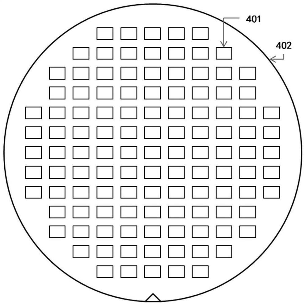
[0042] The present invention provides a three-dimensional fan-out wafer-level packaging method and packaging structure. For the convenience of description, the packaging of a single chip 401 on the wafer 402 will be described below, as shown in figure 1 shown.
[0043] The present invention provides a three-dimensional fan-out wafer-level packaging method, comprising the following steps:
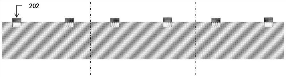
[0044] provide as figure 2 In the shown IC wafer, chip copper pillar bumps 202 are fabricated at chip pin positions through seed layer deposition and electroplating processes, the height of the chip copper pillar bumps is >3 μm, and the structure is as follows: image 3 shown;
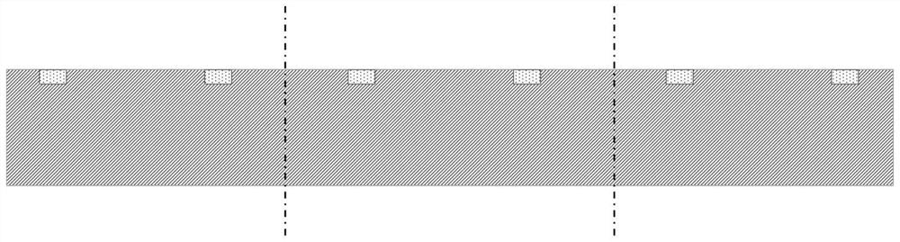
[0045] Divide the IC wafer into single bare chips 201 by mechanical dicing or dry etching, such as Figure 4 shown;
[0046] Provide a glass carrier 301, the surface of the glass carrier 301 is sequentially coated with a temporary bonding laser reaction layer 302 and a temporary bonding glue 303; wherein the thi...
Embodiment 2
[0059] The present invention provides a three-dimensional fan-out wafer-level packaging method, which can realize multi-layer stacking; the specific steps are as follows:
[0060] provide as figure 2 In the shown IC wafer, chip copper pillar bumps 202 are fabricated at chip pin positions through seed layer deposition and electroplating processes, the height of the chip copper pillar bumps is >3 μm, and the structure is as follows: image 3 shown;
[0061] Divide the IC wafer into single bare chips 201 by mechanical dicing or dry etching, such as Figure 4 shown;
[0062] Provide a glass carrier 301, the surface of the glass carrier 301 is sequentially coated with a temporary bonding laser reaction layer 302 and a temporary bonding glue 303; wherein the thickness of the glass carrier 301 is above 100 μm, and the temporary bonding glue The thickness of 303 is more than 1 μm, the thickness of the temporary bonding laser reaction layer 302 is more than 0.1 μm, and the structur...
PUM
| Property | Measurement | Unit |
|---|---|---|
| Height | aaaaa | aaaaa |
| Thickness | aaaaa | aaaaa |
| Thickness | aaaaa | aaaaa |
Abstract
Description
Claims
Application Information
 - Generate Ideas
- Intellectual Property
- Life Sciences
- Materials
- Tech Scout
- Unparalleled Data Quality
- Higher Quality Content
- 60% Fewer Hallucinations
Browse by: Latest US Patents, China's latest patents, Technical Efficacy Thesaurus, Application Domain, Technology Topic, Popular Technical Reports.
© 2025 PatSnap. All rights reserved.Legal|Privacy policy|Modern Slavery Act Transparency Statement|Sitemap|About US| Contact US: help@patsnap.com