
Silicon carbide MOSFET driving circuit, switching power supply and electronic equipment

A drive circuit, silicon carbide technology, applied in high-efficiency power electronic conversion, electrical components, output power conversion devices, etc., can solve problems such as device damage, silicon carbide MOSFET poor negative pressure resistance, etc., to avoid device damage, simplify The effect of circuit structure

Pending Publication Date: 2022-04-26
深圳市恒运昌真空技术有限公司
View PDF0 Cites 2 Cited by
  • Summary
  • Abstract
  • Description
  • Claims
  • Application Information

AI Technical Summary

Problems solved by technology

[0004] Based on this, it is necessary to point out that most of the traditional silicon carbide MOSFET drive circuits are controlled by driving chips with PWM signals. Due to the poor negative pressure resistance of silicon carbide MOSFETs, such designs are prone to generate large di during high-speed switching. / dt (critical current rise rate) acts on the parasitic inductance of the circuit, and the peak voltage generated may cause permanent damage to the device. Provide a silicon carbide MOSFET drive circuit, switching power supply and electronic equipment

Method used


Image

  • Silicon carbide MOSFET driving circuit, switching power supply and electronic equipment
  • Silicon carbide MOSFET driving circuit, switching power supply and electronic equipment
  • Silicon carbide MOSFET driving circuit, switching power supply and electronic equipment

Examples


Embodiment Construction

[0035] In order to facilitate the understanding of the present application, the present application will be described more fully below with reference to the relevant drawings. A preferred embodiment of the application is shown in the drawings. However, the present application can be embodied in many different forms and is not limited to the embodiments described herein. On the contrary, the purpose of providing these embodiments is to make the disclosure of this application more thorough and comprehensive.

[0036] It should be noted that when an element is considered to be "connected" to another element, it may be directly connected to and integrally integrated with the other element, or there may be an intervening element at the same time. The terms "disposition", "one end", "other end" and similar expressions are used herein for the purpose of description only.

[0037] Unless otherwise defined, all technical and scientific terms used herein have the same meaning as commo...


PUM


Abstract

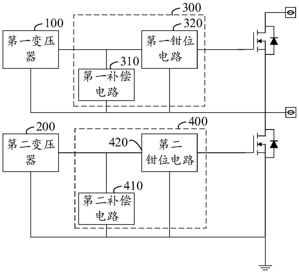
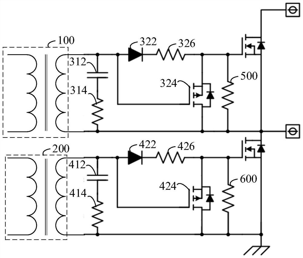
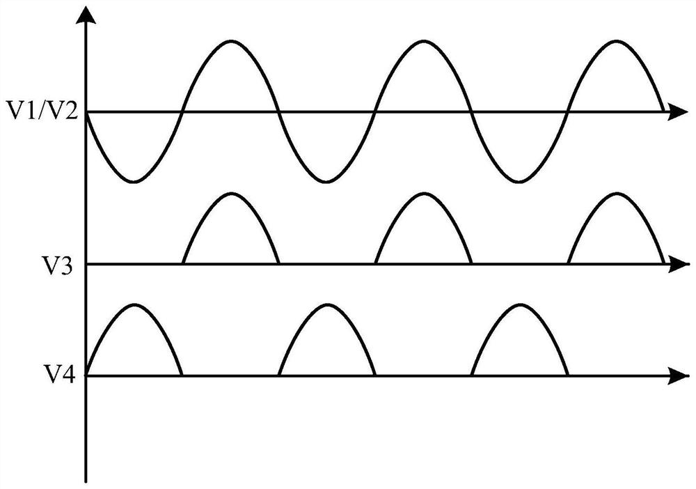
The invention relates to a silicon carbide MOSFET (Metal-Oxide-Semiconductor Field Effect Transistor) driving circuit, a switching power supply and electronic equipment, in the driving circuit, when a received first voltage signal is a positive voltage signal, a first clamping circuit drives a first silicon carbide MOSFET to be conducted; when the received first voltage signal is a negative voltage signal, the first clamping circuit drives the first silicon carbide MOSFET to be disconnected; the second driving circuit comprises a second compensation circuit and a second clamping circuit; when the received second voltage signal is a positive voltage signal, the second clamping circuit drives the second silicon carbide MOSFET to be disconnected; and when the received second voltage signal is a negative voltage signal, the second clamping circuit drives the second silicon carbide MOSFET to be conducted, so that alternate conduction of the two silicon carbide MOSFETs can be realized, the silicon carbide MOSFET driving circuit can work at a megahertz level, the circuit structure is simplified, no voltage spike is generated, the silicon carbide MOSFETs with relatively high gate voltage requirements are effectively protected, and the service life of the silicon carbide MOSFET driving circuit is prolonged. And device damage is avoided.

Description

technical field [0001] The invention relates to the technical field of driving circuits, in particular to a silicon carbide MOSFET driving circuit, a switching power supply and electronic equipment. Background technique [0002] Silicon carbide MOSFET (that is, SiC MOSFET) has the advantages of low Ciss (input capacitance), low Crss (feedback capacitance) and low Ron (on resistance), and can work at power above the MHz (megahertz) level. The existing silicon carbide MOSFET driving methods are basically realized by using the driver chip. The gate voltage signal is generated by supplying power to the driver chip and connected to the PWM signal. According to the number of transistors, it can be divided into single-tube drive and multi-tube drive. According to the number of mode isolation, it can be divided into isolated chip and non-isolated chip. Since the input driving voltage range of SiC MOSFET is -7 / 23V, the symmetric potential is not 0 potential, and the high-frequency d...

Claims


Application Information

Patent Timeline
IPC IPC(8): H02M1/08H02M1/32
CPCH02M1/08H02M1/32Y02B70/10
Inventor 乐卫平林桂浩张桂东
Owner 深圳市恒运昌真空技术有限公司
Learn More