
One-dimensional organic semiconductor nanomaterial with fluorescence response to soman as well as preparation method and application of one-dimensional organic semiconductor nanomaterial

A technology of organic semiconductors and nanomaterials, applied in luminescent materials, organic chemistry, fluorescence/phosphorescence, etc., can solve the problems of low sensitivity and specificity, high cost, complicated operation steps, etc., achieve cheap and easy raw materials, reduce detection The effect of limited, high fluorescence quantum yield

Active Publication Date: 2022-04-29
YANGTZE NORMAL UNIVERSITY
View PDF6 Cites 0 Cited by
  • Summary
  • Abstract
  • Description
  • Claims
  • Application Information

AI Technical Summary

Problems solved by technology

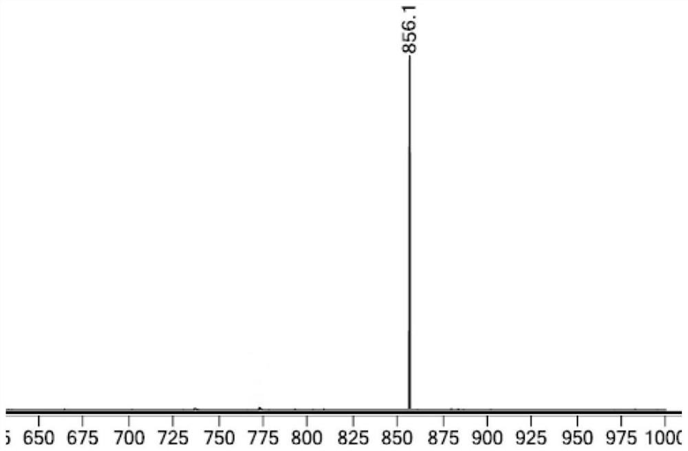
[0005]Aiming at the deficiencies of the above-mentioned prior art, the technical problem to be solved by the present invention is: to provide a novel one-dimensional organic semiconductor nanometer with fluorescence response to Soman The material and its preparation method enrich the types and selectivity of existing nanomaterials; the invention also provides the application of one-dimensional organic semiconductor nanomaterials in Soman detection, which solves the problem of low sensitivity and specificity in existing detection methods, and the operation The steps are complicated and the cost is high

Method used


Image

  • One-dimensional organic semiconductor nanomaterial with fluorescence response to soman as well as preparation method and application of one-dimensional organic semiconductor nanomaterial
  • One-dimensional organic semiconductor nanomaterial with fluorescence response to soman as well as preparation method and application of one-dimensional organic semiconductor nanomaterial
  • One-dimensional organic semiconductor nanomaterial with fluorescence response to soman as well as preparation method and application of one-dimensional organic semiconductor nanomaterial

Examples


Embodiment Construction

[0037] The present invention will be further described in detail in conjunction with the embodiments. The experimental methods used in the following examples are conventional methods unless otherwise specified. The materials and reagents used in the following examples can be obtained from commercial sources unless otherwise specified.

[0038] 1. A method for preparing a one-dimensional organic semiconductor nanomaterial with fluorescence response to Soman

[0039] A synthetic process route of a one-dimensional organic semiconductor nanomaterial with fluorescence response to Soman is as follows:

[0040]

[0041] Specifically include the following steps:

[0042] 1) Preparation of intermediate compound B:

[0043] Take 392mg of compound A and place it in 10g of imidazole, heat it to 130°C, then add 199mg of tridecane-7-amine, react for 1 to 2 hours, then add 100ml of absolute ethanol and 100ml of hydrochloric acid solution with a mass fraction of 36%, and stir Overnight...


PUM


Abstract

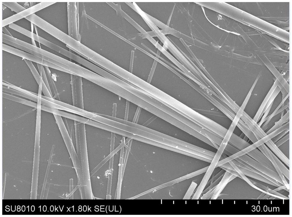
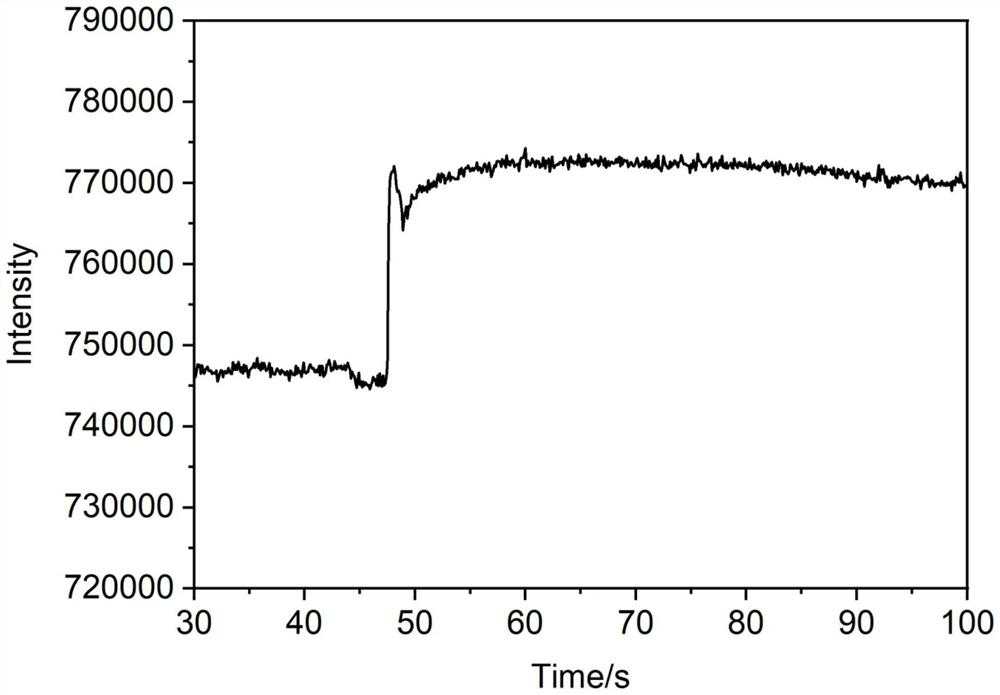
The invention discloses a one-dimensional organic semiconductor nano-material with fluorescence response to soman as well as a preparation method and application thereof. The nano-material is of a strip-shaped nano-structure formed by self-assembly of construction molecules through pi-pi stacking; the one-dimensional organic semiconductor nanomaterial line prepared by the invention has the characteristics of high fluorescence quantum yield, large surface area and the like, has no fluorescence response to phosgene, sarin poison gas, tower collapse poison gas, chlorine, mustard gas and the like, and has good anti-interference capability; the method realizes the detection of the soman specificity and high sensitivity, and has a good application prospect.

Description

technical field [0001] The invention relates to the field of organic semiconductor nanometer materials, in particular to a one-dimensional organic semiconductor nanometer material with fluorescence response to soman. Background technique [0002] Soman is a colorless liquid with a faint fruity aroma, moderate volatility, and its chemical name is isoethyl methylfluorophosphate. In 1944, Dr. Richard Kuhn, a German Nobel laureate, synthesized soman for the first time. The inhalation toxicity of soman is 2-4 times that of sarin, and the skin toxicity is 5-10 times that of sarin. It can be inhaled through the respiratory tract, can also kill humans and animals through skin absorption, or poison food and water sources, and enter the body through the digestive tract. If a person inhales a few mouthfuls of high-concentration soman vapor, he can be fatal within a minute. Another characteristic of Soman is that it has a quick poisoning effect and no specific antidote, so it is know...

Claims


Application Information

Patent Timeline
Patent Type & Authority Applications(China)
IPC IPC(8): C07D471/06C09K11/06G01N21/64
CPCC07D471/06C09K11/06G01N21/6428C09K2211/1044
Inventor 张义斌刘晓玲邱先宇孙林严庆
Owner YANGTZE NORMAL UNIVERSITY
Learn More