Gallium oxide micron column array based on Schottky diode and preparation method thereof

A technology of Schottky diodes and gallium oxide, which is applied in semiconductor/solid-state device manufacturing, semiconductor devices, electrical components, etc., can solve the problem of low breakdown voltage and conduction characteristics, reduced carrier migration rate, and low switching speed. Loss and other issues, to achieve the effect of improving crystal quality, facilitating large-scale integration and use, and avoiding air oxidation

Pending Publication Date: 2022-05-06
NANJING UNIV +1
View PDF0 Cites 0 Cited by
  • Summary
  • Abstract
  • Description
  • Claims
  • Application Information

AI Technical Summary

Problems solved by technology

However, the breakdown voltage and conduction characteristics of the currently studied GaO SBD devices on heterogeneous substrates are far below the expected values ​​of the materials.
[0003] The gallium oxide SBD device described above has the following disadvantages: 1. For the gallium oxide material itself, especially the gallium oxide of the heterogeneous substrate, the dislocation density caused by the lattice mismatch between it and the substrate up to 10 10 cm -2
Usually, dislocations act as carrier trapping centers and scattering centers, forming a leakage path for conductive channels, which severely reduces the carrier mobility
2. The interface state of the existing gallium oxide SBD device has a great influence on the leakage of the device, and its turn-on voltage is very high, which cannot meet the requirements of low turn-on voltage, fast switching speed and low energy loss.

Method used


Image

  • Gallium oxide micron column array based on Schottky diode and preparation method thereof
  • Gallium oxide micron column array based on Schottky diode and preparation method thereof
  • Gallium oxide micron column array based on Schottky diode and preparation method thereof

Examples


Embodiment 1

[0040] Example 1: α-phase gallium oxide microcolumn array based on Schottky diodes

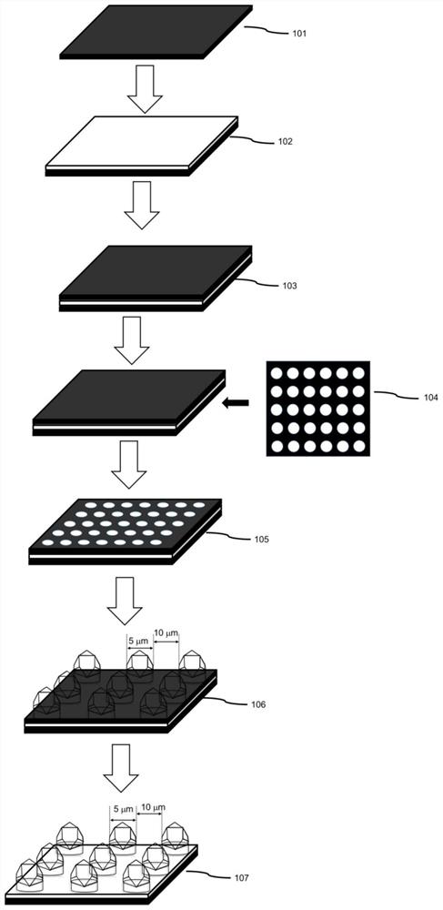
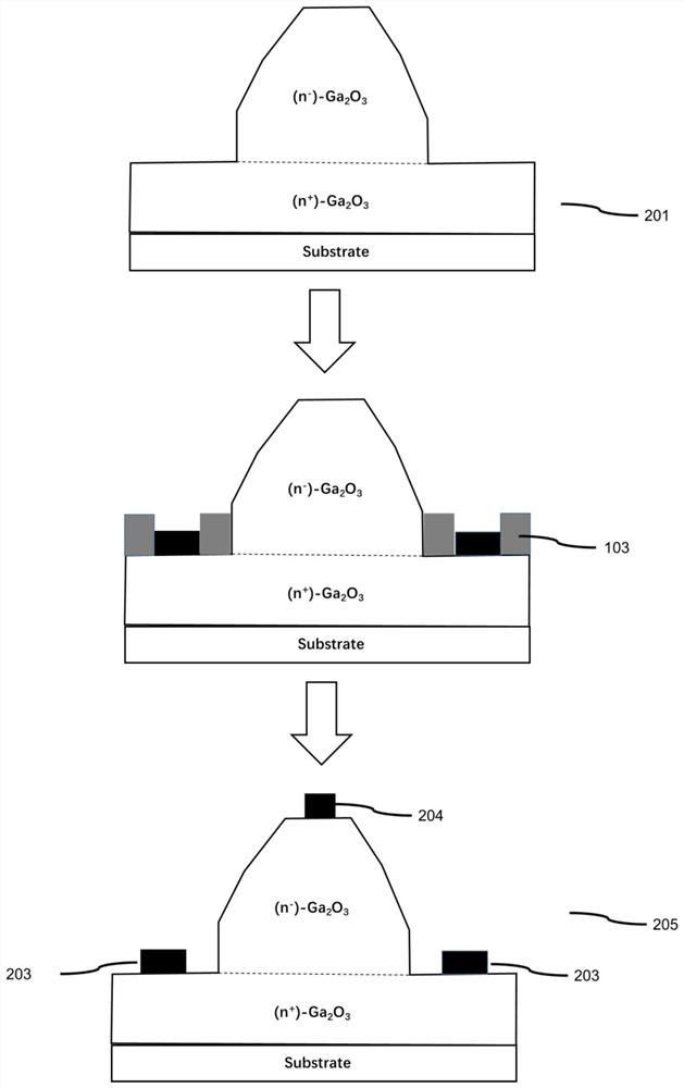
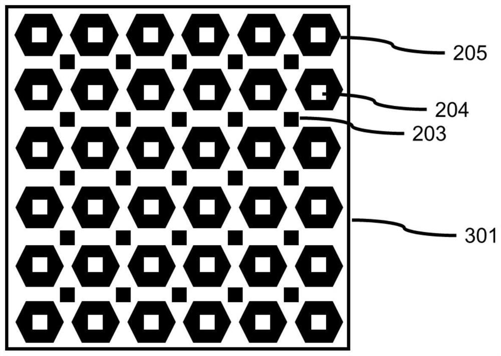
[0041] Such as Figure 1-3As shown, this embodiment is an array of α-phase gallium oxide microcolumns based on Schottky diodes. The Schottky array 301 of the α-phase gallium oxide microcolumn; the Schottky array 301 of the α-phase gallium oxide microcolumn includes the α-phase gallium oxide microcolumn 201, the bottom electrode 203 and the top electrode 204, and the bottom electrode 203 and the top electrode 204 adopt a pair of Multiple structures can independently and accurately control the switching characteristics of each Schottky. The gallium oxide layer 102 is a flat film. The α-phase gallium oxide microcolumn 201 has a hexagonal platform structure, the bottom surface is a hexagon, the top is an equilateral triangle with three corners removed, and the side is composed of three hexagons, three downward-facing pentagons and 6 The α-phase gallium oxide micro-columns 201 have a pore size o...

Embodiment 2

[0055] Example 2: α-phase gallium oxide microcolumn array structure based on κ-phase gallium oxide layer 403

[0056] Such as Figure 4 As shown, the difference from Embodiment 1 is that the gallium oxide layer 102 adopts the κ-phase gallium oxide layer 402 .


PUM

PropertyMeasurementUnit
thicknessaaaaaaaaaa
thicknessaaaaaaaaaa
thicknessaaaaaaaaaa

Abstract

The invention discloses a gallium oxide micron column array based on a Schottky diode and a preparation method of the gallium oxide micron column array. The Schottky diode sequentially comprises a substrate layer, a gallium oxide layer and a Schottky array of gallium oxide micron columns from bottom to top. The gallium oxide layer is made of alpha-phase gallium oxide, kappa-phase gallium oxide, gamma-phase gallium oxide or beta-phase gallium oxide, and the gallium oxide micron columns are made of alpha-phase gallium oxide, kappa-phase gallium oxide, gamma-phase gallium oxide or beta-phase gallium oxide. According to the gallium oxide micron column array Schottky diode, HVPE and Mist CVD are combined, the gallium oxide micron column array is rapidly prepared, a high-quality gallium oxide array material is prepared, and the Schottky diode of the gallium oxide micron column array is low in turn-on voltage, high in switching speed and low in energy loss. Compared with other gallium oxide Schottky diode methods, the gallium oxide micron column array prepared by the method is accurate and controllable in morphology, good in repeatability, high in efficiency and simple in manufacturing process, and effective integration and large-scale production can be realized.

Description

technical field [0001] The invention relates to the technical field of semiconductors, in particular to a schottky diode-based gallium oxide microcolumn array and a preparation method thereof. Background technique [0002] Currently, the ultra-wide bandgap semiconductor gallium oxide (Ga 2 o 3 ) materials have the advantages of wide bandgap, high electron saturation drift velocity, high thermal conductivity, high breakdown electric field strength, and high Ballyga figure of merit compared with Si, GaAs and other materials, and are the preferred materials for advanced power electronic devices. In recent years, gallium oxide Schottky diodes (Ga 2 o 3 SBD) device performance has been improved. In 2016, Japan's FLOSFIA company prepared gallium oxide SBD devices with a withstand voltage of 531V and an on-resistance of only 0.1mΩ cm2; The vertical β-phase gallium oxide SBD device with a withstand voltage of 1076V has a breakdown voltage of 190V and a peak breakdown field str...

Claims


Application Information

Patent Timeline
Patent Type & Authority Applications(China)
IPC IPC(8): H01L29/06H01L29/47H01L29/24H01L29/872H01L21/34
CPCH01L29/0676H01L29/47H01L29/24H01L29/872H01L29/66969
Inventor 叶建东张贻俊任芳芳顾书林张荣
Owner NANJING UNIV
Why Eureka
Try Eureka