Novel micro-strip circulator based on MEMS technology and processing method thereof

A processing method and a technology of a circulator, which are applied in the process for producing decorative surface effects, waveguide devices, metal material coating processes, etc., can solve problems such as high cost and complicated process, and achieve the effect of increasing adhesion

Active Publication Date: 2022-05-06
SOUTHWEST INST OF APPLIED MAGNETICS
View PDF7 Cites 1 Cited by
  • Summary
  • Abstract
  • Description
  • Claims
  • Application Information

AI Technical Summary

Problems solved by technology

[0008] The purpose of the present invention is to provide a new type of microstrip circulator based on MEMS technology to reduce the process steps and complexity of common s

Method used


Image

  • Novel micro-strip circulator based on MEMS technology and processing method thereof
  • Novel micro-strip circulator based on MEMS technology and processing method thereof
  • Novel micro-strip circulator based on MEMS technology and processing method thereof

Examples


Embodiment 1

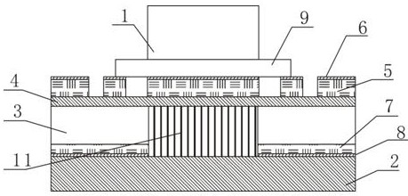
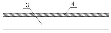
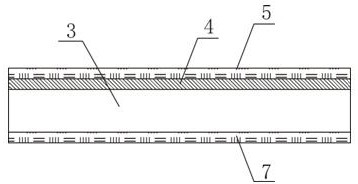
[0054] Embodiment 1: see Figure 1-Figure 6 , a new microstrip circulator based on MEMS technology, including a permanent magnet 1, a dielectric substrate, and an iron substrate 2 arranged in sequence from top to bottom, the dielectric substrate includes a silicon wafer 3 arranged horizontally, and the silicon wafer 3 The upper surface is provided with a polyimide film 4;

[0055] The upper surface of the polyimide film 4 is provided with an upper Cr / Au double-layer film 5, the upper surface circuit is etched on the upper Cr / Au double-layer film 5, and an upper Au plating layer 6 is arranged on the upper surface circuit. Au layer 6 is bonded to permanent magnet 1 through ceramic substrate 9;

[0056] The lower surface of the silicon wafer 3 is also provided with a lower Cr / Au double-layer film 7, and the lower surface circuit is etched on the lower Cr / Au double-layer film 7, and a ferrite groove 10 is also etched in the middle of the silicon wafer 3. Both ends of the ferrite...

Embodiment 2

[0079] Example 2: see Figure 1 to Figure 6 , on the basis of Example 1, we prepared a 5~13GHz microstrip circulator, the best insertion loss is 0.7dB, which matches the design result. Due to the nested structure of the broadband microstrip circulator prepared by this technology, the ferrite magnetization is more uniform than the traditional microstrip circulator, and has better low field loss. Compared with the traditional microstrip circulator in the broadband microstrip circulator devices have clear advantages.

[0080] The thickness of the microstrip circulator prepared by this method is 0.2mm smaller than that of traditional silicon-based MEMS, which reduces the size of the device and meets the development needs of miniaturization.


PUM

PropertyMeasurementUnit
Thicknessaaaaaaaaaa
Thicknessaaaaaaaaaa
Thicknessaaaaaaaaaa

Abstract

The novel micro-strip circulator structurally comprises a permanent magnet, a dielectric substrate and an iron bottom plate which are sequentially arranged from top to bottom, the dielectric substrate comprises a silicon wafer, a polyimide film, an upper Cr/Au double-layer film and an upper Au plating layer are sequentially arranged on the upper surface of the silicon wafer, an upper surface circuit is etched on the upper Cr/Au double-layer film, and a lower surface circuit is etched on the lower Cr/Au double-layer film. The upper Au-plated layer is bonded with the permanent magnet through the ceramic substrate; a lower Cr/Au double-layer film is arranged on the lower surface of the silicon wafer, a lower surface circuit is etched on the lower Cr/Au double-layer film, a ferrite groove is further etched in the middle of the silicon wafer, and a lower Au plating layer is further arranged below the lower surface circuit. According to the novel structure and the processing method provided by the invention, two silicon wafers are not needed, wafer-level metal bonding is not needed, the process steps, the complexity and the cost of the circulator can be effectively reduced, the process redundancy is reduced, the size of the device can be reduced, and the development requirement of miniaturization is met.

Description

technical field [0001] The invention relates to a circulator and a processing method thereof, in particular to a novel microstrip circulator based on MEMS technology and a processing method thereof. Background technique [0002] The circulator is an important basic device in microwave engineering. It is widely used in various civil and military equipment such as civil communication, microwave measurement, radar, communication, electronic countermeasures, and aerospace. It is mainly used to realize the antenna in the equipment. Sending and receiving sharing, inter-level isolation and other issues. At present, microstrip circulators based on silicon-based MEMS technology have the advantages of large carrying power, controllable gyromagnetic area, high processing accuracy, good consistency, high stability, easy integration, and easy debugging, and are gradually starting to be used in some application scenarios. As a substitute for ferrite-based microstrip circulators, it plays...

Claims


Application Information

Patent Timeline
IPC IPC(8): H01P1/38H01P11/00B81C1/00B81B7/02B81B7/00
CPCH01P1/38H01P11/00B81B7/02B81B7/0009B81C1/00222
Inventor 李晓宇高春燕田珺宏胡艺缤张志红
Owner SOUTHWEST INST OF APPLIED MAGNETICS
Why Eureka
Try Eureka