SiC/GaN MOSFET drive circuit and integrated circuit
A driving circuit and circuit technology, applied in the direction of high-efficiency power electronic conversion, electrical components, adjusting electric variables, etc., can solve the problems of negative voltage turn-off peaks, voltage instability, etc. The effect of turning off the negative voltage and turning on to keep the voltage stable
- Summary
- Abstract
- Description
- Claims
- Application Information
AI Technical Summary
Problems solved by technology
Method used
Image

Examples
Embodiment 1
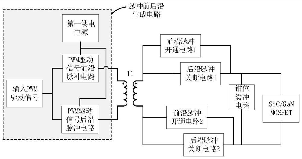
[0077] like figure 1 As shown, this embodiment provides a magnetically isolated SiC / GaN MOSFET drive circuit, including an isolation transformer, a first leading-edge pulse turn-on circuit, a second leading-edge pulse turn-on circuit, a first trailing-edge pulse turn-off circuit, a second trailing-edge pulse Pulse turn-off circuit, clamp buffer circuit, pulse front and rear edge generation circuit and SiC / GaN MOSFET;
[0078] The input end of the first leading edge pulse turn-on circuit and the input end of the first trailing edge pulse turn-off circuit are respectively connected to one end of the secondary side of the isolation transformer;
[0079] The input end of the second leading edge pulse turn-on circuit and the input end of the second trailing edge pulse turn-off circuit are respectively connected to the other end of the secondary side of the isolation transformer;
[0080] One end of the clamp buffer circuit is connected to the output end of the first leading edge ...
Embodiment 2
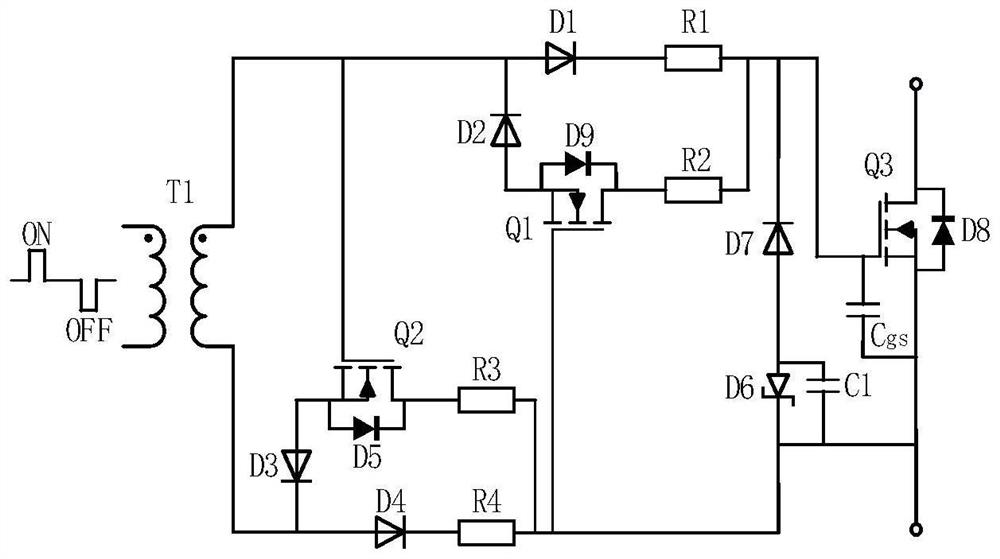
[0109] like Figure 7 As shown, the above secondary side PWM drive signal shaping circuit includes an isolation transformer T1, a first switching tube Q1, a second switching tube Q2 and a driven SiC / GaN switching tube Q3, the first switching tube Q1 and the second switching tube Q2 are both It is a P-channel MOS tube, and the third switching tube Q3 is an N-channel MOS tube; the first diode D1, the second diode D2, the third diode D3, the fourth diode D4, and the fifth and second diodes Diode D5, the sixth diode D6, the seventh diode D7, the eighth diode D8, the ninth diode D9, wherein the first diode D1, the second diode D2, the third and the second The pole diode D3, the fourth diode D4, and the seventh diode D7 are Schottky diodes, and the fifth diode D5, the ninth diode D9, and the eighth diode D8 are respectively the first switching tube Q1 , the body diodes of the second switching tube Q2 and the SiC / GaN switching tube Q3, the sixth diode D6 is a Zener diode; the first ...
Embodiment 3
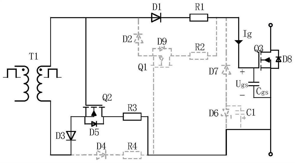
[0116] like Figure 8 As shown, a secondary side PWM drive signal shaping circuit can adjust the turn-on and turn-off voltage values of the driven SiC / GaN switch, including the isolation transformer T1, the first switch Q1, the second switch Q2 and the driven SiC / GaN switch tube Q3, the first switch tube Q1 and the second switch tube Q2 are N-channel MOS tubes; the first diode D1, the second diode D2, the third diode D3, and the fourth diode Tube D4, fifth diode D5, sixth diode D6, seventh diode D7, eighth diode D8, ninth diode D9, wherein the first diode D1, the second diode The tube D2, the third diode D3, and the fourth diode D4 are Schottky diodes, and the fifth diode D5, the ninth diode D9, and the eighth diode D8 are respectively the second switching tubes Q2, The body diodes of the first switching tube Q1 and the SiC / GaN switching tube Q3, the sixth diode D6 is a Zener diode, and the seventh diode D7 is a Zener diode; the first resistor R1, the second resistor R2, t...
PUM
 Abstract
Description
Claims
Application Information
 - R&D
- Intellectual Property
- Life Sciences
- Materials
- Tech Scout
- Unparalleled Data Quality
- Higher Quality Content
- 60% Fewer Hallucinations
Browse by: Latest US Patents, China's latest patents, Technical Efficacy Thesaurus, Application Domain, Technology Topic, Popular Technical Reports.
© 2025 PatSnap. All rights reserved.Legal|Privacy policy|Modern Slavery Act Transparency Statement|Sitemap|About US| Contact US: help@patsnap.com