RESFET device and preparation method thereof

A device and MOS tube technology, applied in the field of RESFET devices and their preparation, can solve the problems of large volume, insufficient integration, high energy consumption, etc., and achieve the effects of reducing device volume, improving device performance, and low static power consumption

Pending Publication Date: 2022-05-13
SHENZHEN UNIV
View PDF0 Cites 0 Cited by
  • Summary
  • Abstract
  • Description
  • Claims
  • Application Information

AI Technical Summary

Problems solved by technology

[0006] The purpose of the present invention is to provide a RESFET device to solve the technical probl

Method used


Image

  • RESFET device and preparation method thereof

Examples


Embodiment Construction

[0059] In order to make the technical problems, technical solutions and beneficial effects to be solved by the present invention clearer, the present invention will be further described in detail below in conjunction with the embodiments. It should be understood that the specific embodiments described here are only used to explain the present invention, not to limit the present invention.

[0060] In the embodiments of the present invention, the following nouns are described as follows.

[0061]MOCVD method: MOCVD uses organic compounds of group III and group II elements and hydrides of group V and group VI elements as crystal growth source materials, and performs vapor phase epitaxy on the substrate by thermal decomposition reaction to grow various III-V Thin-layer single-crystal materials of main group, II-VI subgroup compound semiconductors and their multiple solid solutions.

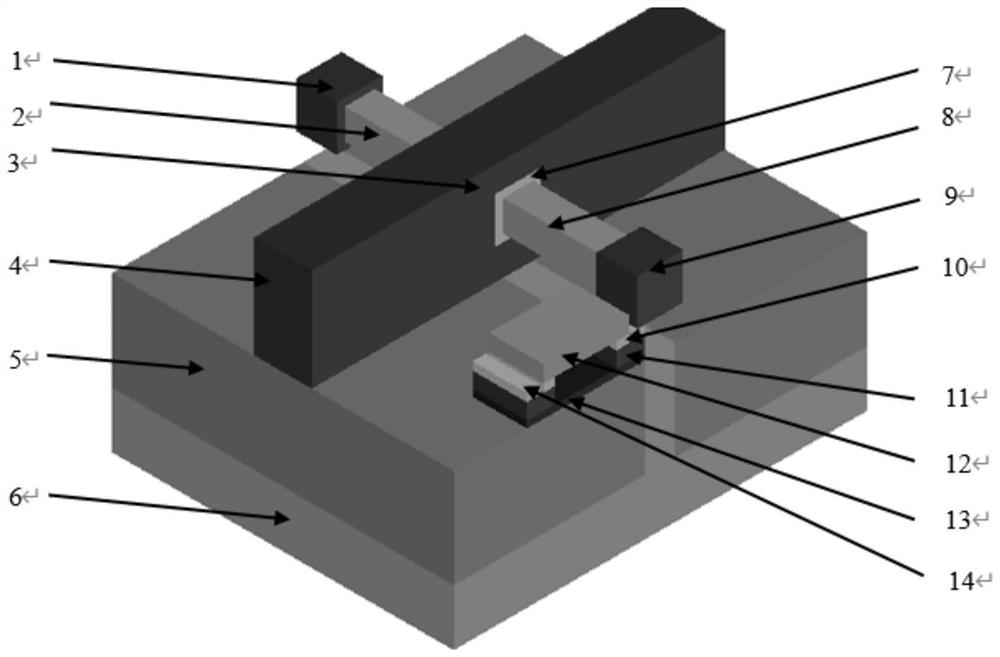
[0062] One aspect of the present invention provides a RESFET device, comprising:

[0063] MOS t...


PUM

PropertyMeasurementUnit
Thicknessaaaaaaaaaa
Widthaaaaaaaaaa
Thicknessaaaaaaaaaa

Abstract

According to the RESFET device and the preparation method thereof, compared with the prior art, the static power consumption of the RESFET device is lower, the time delay is lower, the size of the device is reduced, and the integration level is improved. The upper surface, the lower surface and the side surface of the nanowire are all provided with the channels, so that a multi-layer channel structure can be formed, and the overall carrier mobility of the channel structure of the multi-layer nanowire laminated ring gate and the comprehensive performance of the multi-layer nanowire are further improved. Due to the fact that the nanowire with the narrow width is adopted, the characteristic of low power consumption is achieved. Compared with a traditional vertical FinFET device, more effective heat dissipation, longer-time normal work and higher output current density can be achieved. According to the manufacturing method of the RESFET device, the performance of the device is improved, the integration level of the device is improved, energy consumption is reduced, meanwhile, technical means without any threshold is adopted, and therefore the manufacturing method is suitable for large-scale application and popularization.

Description

technical field [0001] The invention belongs to the field of device manufacturing in semiconductor technology, and in particular relates to a RESFET device and a preparation method thereof. Background technique [0002] GaN-based materials have a series of material performance advantages such as large bandgap width, high breakdown field strength, high polarization coefficient, high electron mobility and electron saturation drift speed, and are the preferred materials for the preparation of a new generation of high-performance power electronic devices. application prospects. GaN-based materials are very attractive for both optoelectronic and microelectronic devices. GaN-based materials have the characteristics of forbidden bandwidth, high breakdown voltage, high electron saturation drift velocity, and good thermal stability, and can form an ideal heterojunction with AlGaN alloy materials, and the large conduction band shift on the heterointerface and the The high piezoelect...

Claims


Application Information

Patent Timeline
IPC IPC(8): H01L29/10H01L29/78H01L23/64H01L27/06H01L21/336H01L21/8252B82Y40/00
CPCH01L29/785H01L27/0635H01L28/20H01L29/66522H01L29/66795H01L29/1037B82Y40/00H01L21/8252
Inventor 黄双武高麟飞林峰吴钧烨宋利军黎晓华刘新科
Owner SHENZHEN UNIV
Why Eureka
Try Eureka