Multi-cavity PVD-RTA mixed film deposition system
A PVD-RTA, thin film deposition technology, applied in the field of ion sputtering deposition system, can solve the problem of not being able to give full play to the role of RTA, reduce equipment use and maintenance costs, reduce temperature requirements, and improve the effect of thin film crystal structure
- Summary
- Abstract
- Description
- Claims
- Application Information
AI Technical Summary
Problems solved by technology
Method used
Image

Examples
Embodiment Construction
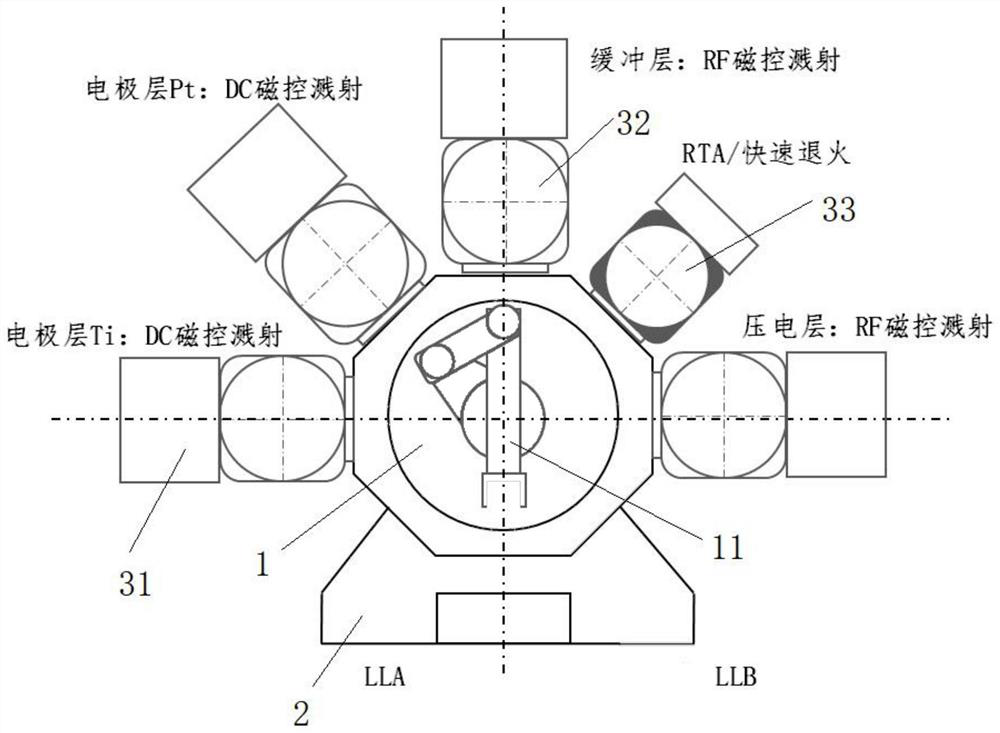
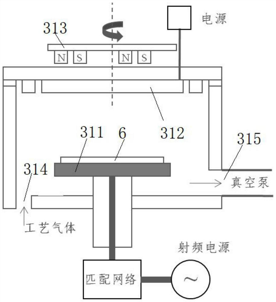
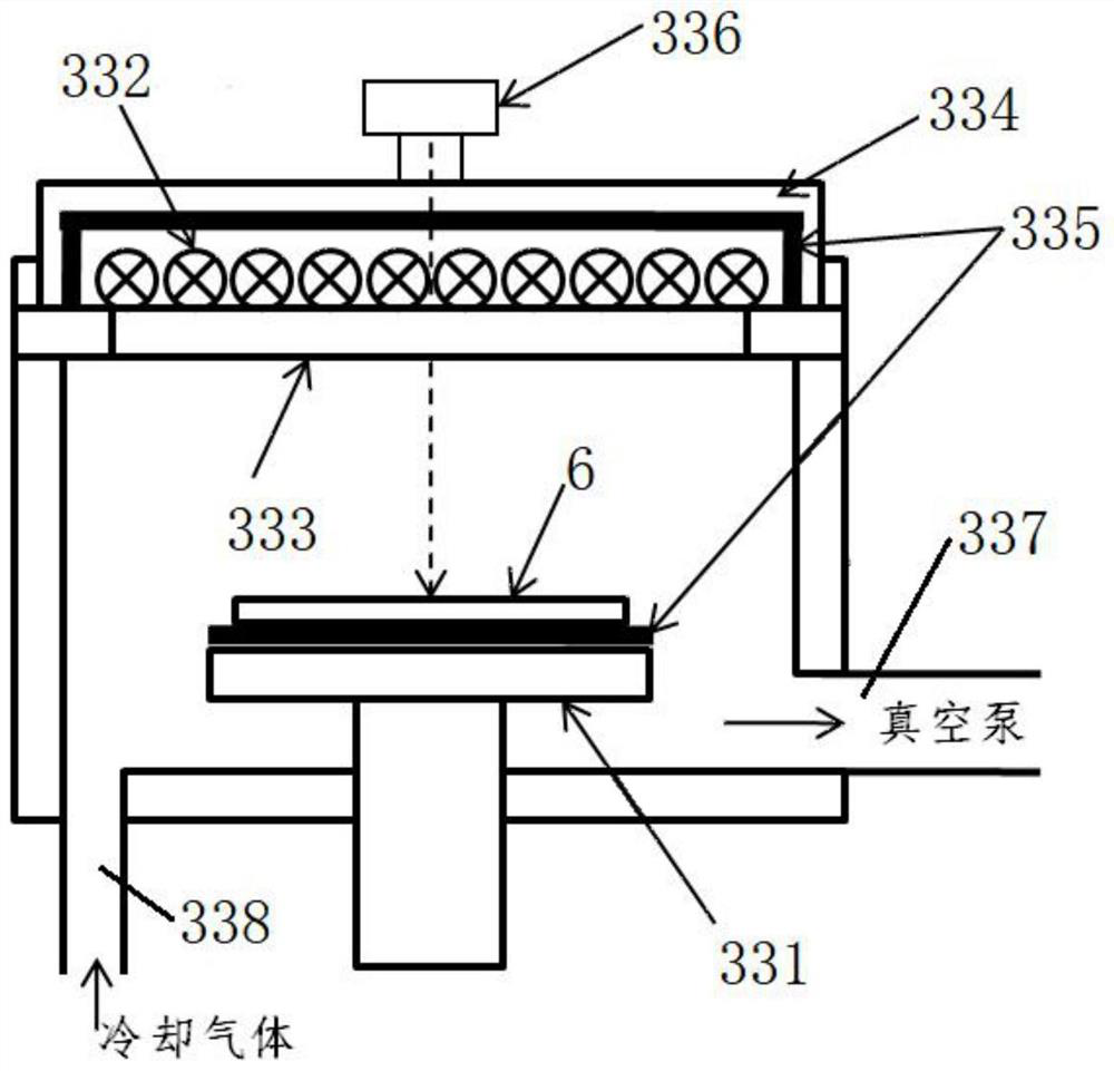
[0044] refer to Figure 1 to Figure 6 The embodiment of the multi-cavity PVD-RTA hybrid thin film deposition system of the present invention will be further described.
[0045] In the description of the present invention, it should be noted that for orientation words, such as the term "center", "horizontal (X)", "longitudinal (Y)", "vertical (Z)", "length", " Width", "Thickness", "Top", "Bottom", "Front", "Back", "Left", "Right", "Vertical", "Horizontal", "Top", "Bottom", "Inner ", "outside", "clockwise", "counterclockwise" and other indication orientations and positional relationships are based on the orientation or positional relationship shown in the drawings, and are only for the convenience of describing the present invention and simplifying the description, rather than indicating or implying the Means that a device or element must have a specific orientation, be constructed and operated in a specific orientation should not be construed as limiting the specific protectio...
PUM
 Abstract
Description
Claims
Application Information
 - Generate Ideas
- Intellectual Property
- Life Sciences
- Materials
- Tech Scout
- Unparalleled Data Quality
- Higher Quality Content
- 60% Fewer Hallucinations
Browse by: Latest US Patents, China's latest patents, Technical Efficacy Thesaurus, Application Domain, Technology Topic, Popular Technical Reports.
© 2025 PatSnap. All rights reserved.Legal|Privacy policy|Modern Slavery Act Transparency Statement|Sitemap|About US| Contact US: help@patsnap.com