Vertically-arranged MSM capacitor structure and manufacturing method thereof

A technology of capacitor structure and vertical layout, which is applied in the gold field to reduce costs and control risks, and overcome the effect of three-dimensional integration of capacitors that cannot be integrated

Active Publication Date: 2022-05-31
10TH RES INST OF CETC
View PDF11 Cites 0 Cited by
  • Summary
  • Abstract
  • Description
  • Claims
  • Application Information

AI Technical Summary

Problems solved by technology

However, compared with the extension in the Z direction, the main contradiction of chip or module miniaturization is still concentrated in the XY plane layout
Compared with type 1) capacitor form, although the type 2) and 3) capacitor form can reduce the area occupied by the plane layout to a certain extent in the field of small and medium capacitance applications, and improve the miniaturization performance, the calculation formula of the plate capacitance Limits the size of

Method used


Image

  • Vertically-arranged MSM capacitor structure and manufacturing method thereof
  • Vertically-arranged MSM capacitor structure and manufacturing method thereof
  • Vertically-arranged MSM capacitor structure and manufacturing method thereof

Examples


Embodiment 1

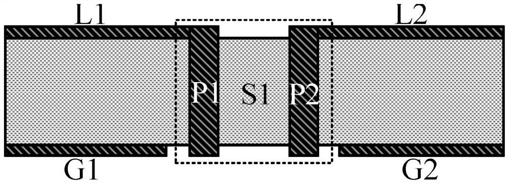
[0019] In the vertical MSM capacitor body structure, the two flat metallized through grooves, blind grooves or buried grooves are in a parallel relationship with each other. The sidewalls of the flat metallized through grooves, blind grooves or buried grooves can be metallized hollow structures or fully filled with metal. solid structure. The dielectric partition wall S1 can be a semiconductor dielectric layer sandwiched between two flat metallized through grooves, blind grooves or buried grooves and adjacent to the sidewalls. The semiconductor dielectric layer and the semiconductor dielectric substrate where it is located are of the same material and integrated Connect the capacitor terminal. L1 and L2 can be in the form of transmission lines such as microstrip line, stripline, coplanar waveguide, etc. The metal layers G1 and G2 that are not in communication with the capacitor plates can be used as ground or otherwise.

Embodiment 2

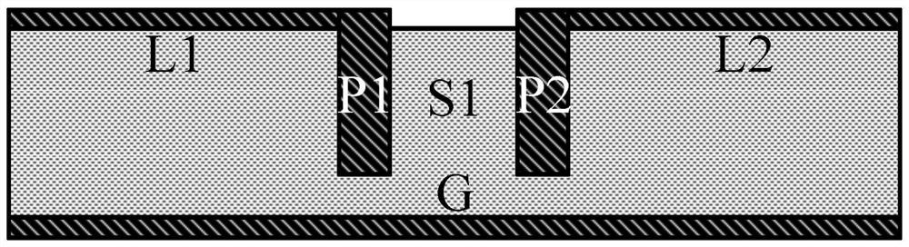
[0021] see image 3 . The difference between this embodiment and Embodiment 1 is that the two parallel grooves are buried grooves, that is, one end of the grooves does not extend to communicate with the metal layer. The difference between this embodiment and the process steps of Embodiment 1 is that the process step of performing a buried trench-to-through trench conversion using a backside chemical mechanical polishing CMP process can be omitted.

Embodiment 3

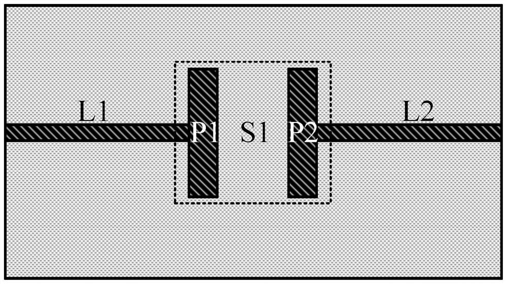
[0023] Figure 4 , Figure 5 It is a schematic front view of the vertical metal-semiconductor-metal MSM capacitor structure connected in series and parallel in an actual circuit, that is, as a demonstration of the actual layout usage of the capacitor structure. The series connection mode is characterized in that, as shown in Embodiment 1, the two capacitor lead-out ends are respectively connected to two parallel metal plate grooves, and the two lead-out ends can be located in the same metal layer, or can be located in different metal layers up and down. The grooves of the parallel metal plates are not connected. The parallel connection method is characterized in that the two capacitor lead-out ends are connected to one of the parallel metal plate grooves, the two lead-out ends can be located in the same metal layer, or can be located in different metal layers up and down, and the other parallel metal plate groove is connected to the ground end. This embodiment exemplifies t...


PUM


Abstract

The vertically-arranged MSM capacitor structure and the manufacturing method thereof disclosed by the invention can be applied to various semiconductor integration/packaging structures with small and medium capacitance values and miniaturization requirements. The structure comprises two flat metalized through grooves or blind grooves inserted into a semiconductor dielectric substrate, and the two flat metalized through grooves, blind grooves or buried grooves which are perpendicular to the surface of the semiconductor dielectric substrate and are separated by a dielectric partition wall S1 are formed in specific positions of the semiconductor dielectric substrate. A dielectric partition wall of a vertically-arranged MSM capacitor structure is perpendicular to the upper surface and the lower surface of the semiconductor dielectric substrate to form a dielectric layer of the capacitor. Two parallel rectangular through grooves, blind grooves or buried grooves are embedded with metal electrode plates P1 and P2 which form homoepitaxy of a capacitor body, and the two metal electrode plates extend to two ends of a dielectric partition wall S1 through a metal layer microstrip connecting line etched on the surface of a semiconductor dielectric substrate to form an electrode structure led out from leading-out ends L1 and L2 of the MSM capacitor. Therefore, a vertically-arranged MSM capacitor equivalent circuit structure is formed.

Description

technical field [0001] The invention relates to the fields of microwave technology and wireless communication technology, an embedded integrated three-dimensional flat plate capacitor structure, in particular a representative metal-semiconductor- Metal (MSM), ie MSM=metal-semiconductor-metal vertical capacitor structure, and also relates to a manufacturing method of the MSM capacitor. Background technique [0002] In the current 2D / 2.5D / 3D integrated circuit / package design, capacitors with different capacitance values ​​and packages are widely used in functional links such as decoupling, bypass, DC blocking, resonance, and energy storage. Existing capacitor forms mainly include: 1) electrolytic capacitors, tantalum capacitors, monolithic capacitors, ceramic capacitors, etc. traditionally installed on the surface of the plate or package; 2) small and medium-sized capacitors installed in the cavity for easy interconnection or gold wire bonding Capacitance chip capacitors; 3) ...

Claims


Application Information

Patent Timeline
IPC IPC(8): H01L23/64
CPCH01L28/40H01L28/90
Inventor 祁冬张睿张先荣王志辉朱勇
Owner 10TH RES INST OF CETC
Why Eureka
Try Eureka