Photoelectric integrated device and preparation method

An integrated device and optoelectronic integration technology, applied in the field of integrated optoelectronics, can solve the problems of large electronic transistor circuits, etc., and achieve the effects of improving performance and integration, fast speed, and saving area

Pending Publication Date: 2022-06-03
NANJING UNIV OF POSTS & TELECOMM
View PDF0 Cites 0 Cited by
  • Summary
  • Abstract
  • Description
  • Claims
  • Application Information

AI Technical Summary

Problems solved by technology

[0004] The purpose of the present invention is to provide an optoelectronic integrated device and its preparation method, so as to solve the defect that the existing electronic transistor circuits are all based on the silicon-based platform and have a large volume.

Method used


Image

  • Photoelectric integrated device and preparation method
  • Photoelectric integrated device and preparation method
  • Photoelectric integrated device and preparation method

Examples


Embodiment Construction

[0016] In order to make the technical means, creative features, achievement goals and effects realized by the present invention easy to understand, the present invention will be further described below with reference to the specific embodiments.

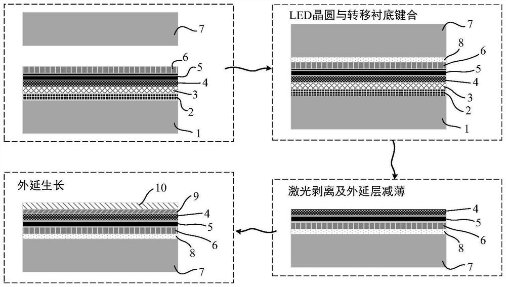
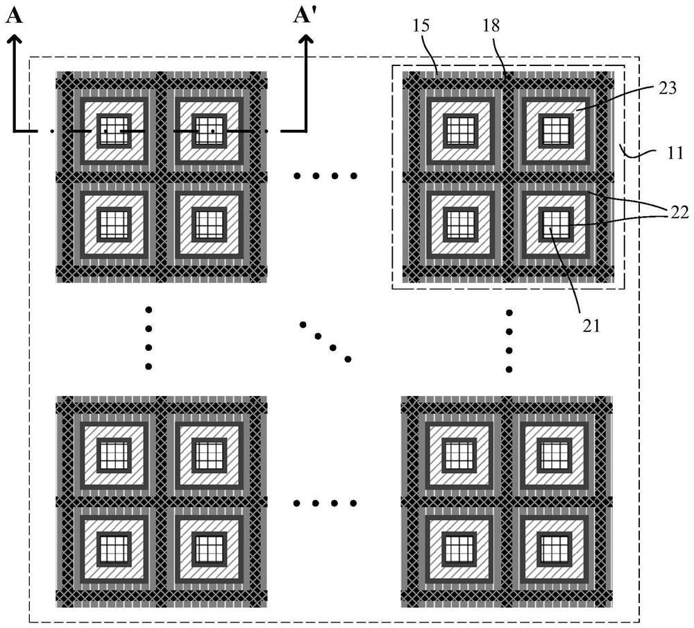
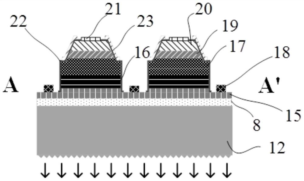
[0017] see Figure 1-4 , the present invention proposes an optoelectronic integrated device, comprising:

A plurality of orderly arranged basic units 11, the basic units 11 include a multi-quantum well Micro LED 13 and a vertical structure GaN MOSFET 14;

The sapphire substrate 12, the top layer of the sapphire substrate 12 is provided with a bonding medium layer 8, and the bottom layer of the sapphire substrate 12 is the light emitting surface of the device; the bottom surface of the sapphire adopts a patterned structure to reduce the reflection of incident light, thereby Improve light output efficiency;

The multi-quantum well Micro LED 13 is arranged on the top layer of the bonding dielectric layer 8; the vertical structure GaN ...


PUM

PropertyMeasurementUnit
angleaaaaaaaaaa

Abstract

The invention discloses a photoelectric integrated device and a manufacturing method thereof, and the device comprises a plurality of basic units which are arranged in order, and each basic unit comprises a multi-quantum well MicroLED and a vertical structure GaN MOSFET; the top layer of the sapphire substrate is provided with a bonding dielectric layer, and the bottom layer of the sapphire substrate is a light emitting surface of the device; the multi-quantum well Micro LED is arranged on the top layer of the bonding dielectric layer; the GaN MOSFET with the vertical structure is arranged above the multi-quantum well Micro LED, and a drain region of the GaN MOSFET with the vertical structure is connected in series with an N region of the multi-quantum well Micro LED through a shared diode N-GaN structure layer; the light-emitting device and the driving electronic device are manufactured on the same chip, batch manufacturing can be achieved through an existing GaN process platform, the production cost is reduced, and the light-emitting device and the driving electronic device have the remarkable advantages of being small in size, high in speed and high in reliability. The GaN MOSFET adopts a novel vertical structure design, so that the channel length of a driving transistor can be greatly shortened, and the GaN MOSFET has important significance in improving the performance and the integration level of an integrated device.

Description

technical field [0001] The invention relates to an optoelectronic integrated device and a preparation method, belonging to the technical field of integrated optoelectronics. Background technique [0002] The band gaps of III-V semiconductors GaN and its alloys cover the spectral range from infrared to visible light, and have achieved great success in solid-state lighting, displays, high-density storage, and underwater communications. At the same time, GaN-based transistor technology has also received attention from the industry in recent years, and has developed rapidly, showing attractive application prospects in high-power and high-frequency devices. At present, the research of GaN in optoelectronic technology and electronic technology is independent of each other, and in practical applications, optoelectronic technology is inseparable and interdependent with electronic technology. For example, GaN light-emitting diodes (LEDs) must be driven by electronic transistor circui...

Claims


Application Information

Patent Timeline
Patent Type & Authority Applications(China)
IPC IPC(8): H01L27/15H01L33/00H01L21/336
CPCH01L27/153H01L33/0075H01L33/0066H01L29/66522H01L33/0093
Inventor 严嘉彬石帆杨凌云吴洁戴叶玲
Owner NANJING UNIV OF POSTS & TELECOMM
Why Eureka
Try Eureka