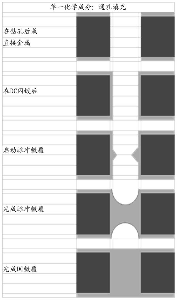
Single-step electrolytic method for filling through-holes in printed circuit boards and other substrates
A technology for printed circuit boards and electronic substrates, applied in the directions of printed circuits, printed circuit manufacturing, printed circuit components, etc., and can solve problems such as circuit failures
- Summary
- Abstract
- Description
- Claims
- Application Information
AI Technical Summary
Problems solved by technology
Method used
Image

Examples
Embodiment
[0139] The acid copper plating bath was prepared according to the following parameters:
[0140] Element constitute Control range copper sulfate 240g / L 230g / L-245g / L sulfuric acid 90g / L 85g / L-90g / L Chloride 75ppm 70ppm-100ppm brightener 7ppm 4ppm-10ppm wetting agent 5g / L 1g / L-10g / L leveling agent 10ppm 0.001ppm-50ppm bath temperature 23℃ 22℃-25℃
[0141] The concentration of copper sulfate is maintained by the addition of copper oxide on a manual or automatic basis based on operational amperometric analysis and / or with chemical titration analysis.
[0142] Supplement the concentration of sulfuric acid and chloride ions based on chemical titration analysis.
[0143] Replenishment of brighteners, wetting agents, and leveling agents is accomplished using an automated drug delivery system based on operational amperometric and / or cyclic voltammetric stripping (CVS) analysis.
Embodiment 1
[0150] The acid copper plating baths described above were used to plate test panels using plating cycles in accordance with the present invention and the plating parameters outlined in Table 4.
[0151] A cycle time of 80 minutes was used to plate a test panel with a thickness of 0.075 mm and a 0.12 mm laser drilled through hole.
[0152] The current density is 2.2A / dm 2 And the plating was performed for 80 minutes.
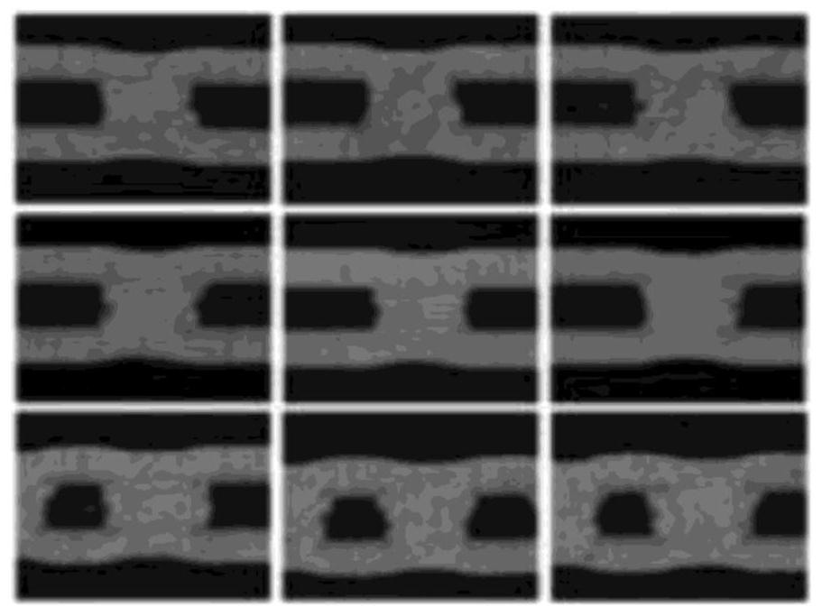
[0153] image 3 A cross section of a plated circuit board is depicted and shows 23 to 25 micron plated deposits and no pits.
Embodiment 2
[0160] The acid copper plating baths described above were used to plate test panels using plating cycles in accordance with the present invention and the plating parameters outlined in Table 4.
[0161] A 60 minute cycle time was used to plate test panels having a thickness of 0.07 mm and mechanical means to form 0.1 mm through holes therein.
[0162] The current density is 2.2A / dm 2 And the plating was performed for 60 minutes.
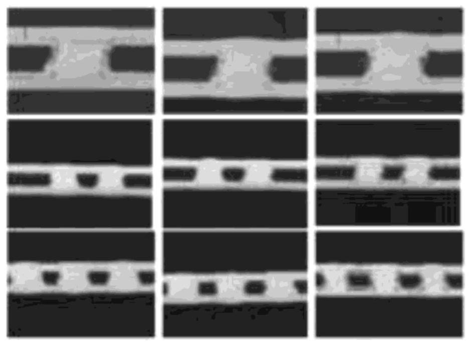
[0163] Figure 5 A cross section of a plated circuit board is depicted and shows 18 to 20 micron plated deposits and no pits.
PUM
| Property | Measurement | Unit |
|---|---|---|
| thickness | aaaaa | aaaaa |
| diameter | aaaaa | aaaaa |
| diameter | aaaaa | aaaaa |
Abstract
Description
Claims
Application Information
 - R&D
- Intellectual Property
- Life Sciences
- Materials
- Tech Scout
- Unparalleled Data Quality
- Higher Quality Content
- 60% Fewer Hallucinations
Browse by: Latest US Patents, China's latest patents, Technical Efficacy Thesaurus, Application Domain, Technology Topic, Popular Technical Reports.
© 2025 PatSnap. All rights reserved.Legal|Privacy policy|Modern Slavery Act Transparency Statement|Sitemap|About US| Contact US: help@patsnap.com