Wafer bonding method and preparation method or packaging method of semiconductor device

A wafer bonding and bonding technology, applied in the field of semiconductor technology, can solve problems such as bonding failure and bonding bubbles, and achieve the effect of improving yield and avoiding bonding failure.

Pending Publication Date: 2022-06-24
GTA SEMICON CO LTD
View PDF0 Cites 0 Cited by
  • Summary
  • Abstract
  • Description
  • Claims
  • Application Information

AI Technical Summary

Problems solved by technology

[0003] Bonding glue is one of the common methods of wafer bonding, but when coating the bonding glue during wafer bonding, there will be covering gaps when deep grooves are encountered, resulting in the problem of bonding bubbles, and the bubbles will It is easy to make the bond fail, so the traditional method of wafer bonding utilizes complementary methods, such as figure 1 The method shown uses double-sided glue coating, that is, the bonding glue is coated on the front surface of the wafer composed of the substrate layer 1011 of the wafer to be bonded, the epitaxial layer 1012 of the wafer to be bonded, and the imprinted pattern layer 102 of the wafer to be bonded. At the same time as 103, the bonding adhesive 104 is also coated on the bonding carrier 105. Even if there are bubbles on the side of the wafer coated with the bonding adhesive 103, the bonding adhesive 104 on the carrier will be filled in during the bonding process to eliminate bonding bubbles
However, the above-mentioned method of eliminating bonding air bubbles is to eliminate the air bubbles in a repairing way after the air bubbles are generated, without solving the problem of air bubbles in the wafer bonding process from the root cause of the air bubbles, that is, the generation of step differences.

Method used


Image

  • Wafer bonding method and preparation method or packaging method of semiconductor device
  • Wafer bonding method and preparation method or packaging method of semiconductor device
  • Wafer bonding method and preparation method or packaging method of semiconductor device

Examples


Embodiment 1

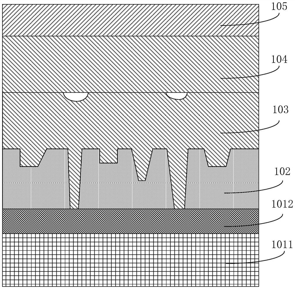
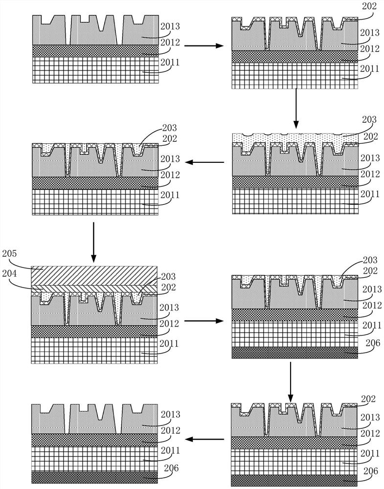
[0078] like image 3 As shown, this embodiment provides a method for wafer bonding. The wafer to be bonded 201 is a silicon carbide wafer having an engraved pattern layer 2013 that has been photoetched on one side, and the wafer to be bonded 201 includes a silicon carbide liner. Bottom 2011 , epitaxial layer 2012 and imprint pattern layer 2013 .

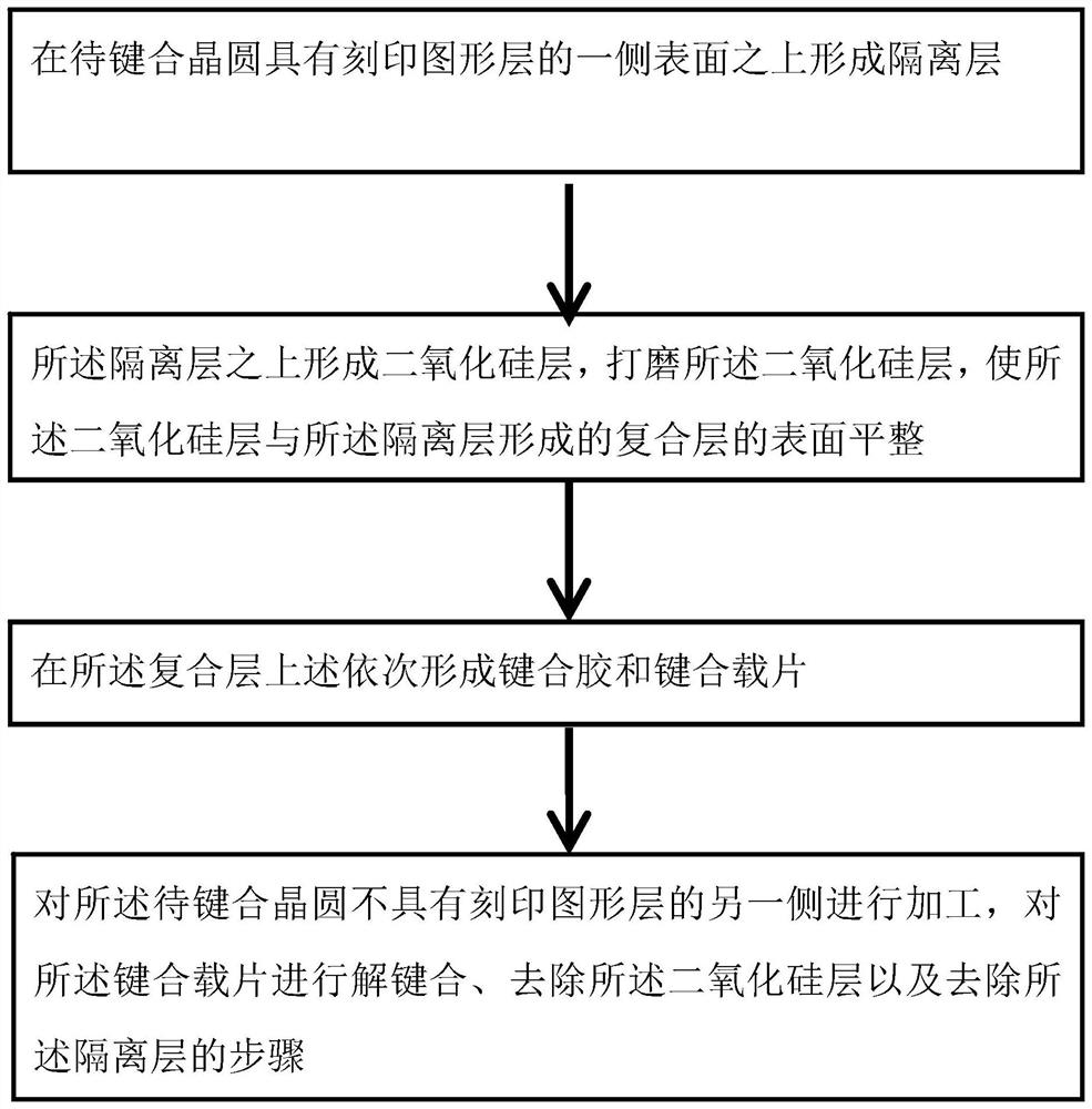
[0079] Step S10 : coating a polyimide with a thickness of 1 μm on the side of the wafer to be bonded 201 with the imprinted pattern layer 2013 to form the isolation layer 202 ;

[0080]Step S20: A silicon dioxide layer 203 is grown on the isolation layer 202 by using ethyl orthosilicate as a raw material by plasma enhanced chemical vapor deposition, and chemical mechanical polishing is used to remove excess silicon dioxide material, so that the silicon dioxide layer 203 is isolated from the Layer 202 is in the same plane to prepare a composite layer;

[0081] Step S30: forming a 20 μm bonding adhesive layer 204 and a bonding carrie...


PUM

PropertyMeasurementUnit
thicknessaaaaaaaaaa
thicknessaaaaaaaaaa
tensile strengthaaaaaaaaaa

Abstract

The invention discloses a wafer bonding method and a preparation method or a packaging method of a semiconductor device. The wafer bonding method comprises the following steps: step S10, forming an isolation layer on the surface of one side of a wafer to be bonded, which is provided with an engraved pattern layer; s20, forming a silicon dioxide layer on the isolation layer, and polishing the silicon dioxide layer to enable the surface of a composite layer formed by the silicon dioxide layer and the isolation layer to be smooth; and S30, sequentially forming a bonding glue layer and a bonding slide on the composite layer. According to the bonding method, the isolation layer and the silicon dioxide layer are sequentially formed, and the silicon dioxide material is firstly formed on the isolation layer and is ground to be flush with the highest surface of the isolation layer, so that the problem can be effectively solved through the step difference which is a root cause of generation of bonding bubbles in the bonding process; and the problem of bonding failure in the wafer bonding process can be further avoided. By using the wafer bonding method, the yield of semiconductor device preparation and packaging can be effectively improved.

Description

technical field [0001] The invention relates to the field of semiconductor technology, in particular to a wafer bonding method and a preparation method or packaging method of a semiconductor device. Background technique [0002] Wafer bonding is an emerging microelectronics manufacturing technology, which refers to the close bonding of two mirror-polished homogeneous or heterogeneous wafers through chemical and physical action. After the wafers are bonded, the atoms at the interface are subjected to external forces. Act to produce a reaction to form a covalent bond into a whole, and make the bonding interface reach a specific bonding strength. Therefore, it is widely used in material preparation, three-dimensional microstructure integration and integrated circuit (IC), microelectromechanical system (MEMS) device manufacturing and packaging. In addition, wafer bonding technology is also used to make electrodes and cavities in many microelectromechanical systems (MEMS) compon...

Claims


Application Information

Patent Timeline
Patent Type & Authority Applications(China)
IPC IPC(8): H01L21/762H01L21/60
CPCH01L21/76229H01L24/27H01L2224/271
Inventor 魏丹珠
Owner GTA SEMICON CO LTD
Why Eureka
Try Eureka