
Preparation method of CMOS phase inverter based on GaOx-NMOS/GaN-PMOS

A channel layer and buffer layer technology, applied in the field of materials, can solve the problems of device performance impact, poor heat dissipation, complex circuit, etc., and achieve the effect of good heat dissipation and simple structure

Pending Publication Date: 2022-07-08
SHENZHEN UNIV
View PDF0 Cites 0 Cited by
  • Summary
  • Abstract
  • Description
  • Claims
  • Application Information

AI Technical Summary

Problems solved by technology

[0003] However, the existing inverters have high power consumption, complex manufacturing process, complex circuits, poor heat dissipation, and the maximum on-state current density is limited to tens of mA / mm. The size of the device is relatively large, and the production process of the device usually requires plasma Body etching will have a relatively large impact on device performance

Method used


Image

  • Preparation method of CMOS phase inverter based on GaOx-NMOS/GaN-PMOS
  • Preparation method of CMOS phase inverter based on GaOx-NMOS/GaN-PMOS
  • Preparation method of CMOS phase inverter based on GaOx-NMOS/GaN-PMOS

Examples


Embodiment Construction

[0023] In order for those skilled in the art to better understand the solutions of the present invention, the technical solutions in the embodiments of the present invention will be clearly and completely described below with reference to the accompanying drawings in the embodiments of the present invention.

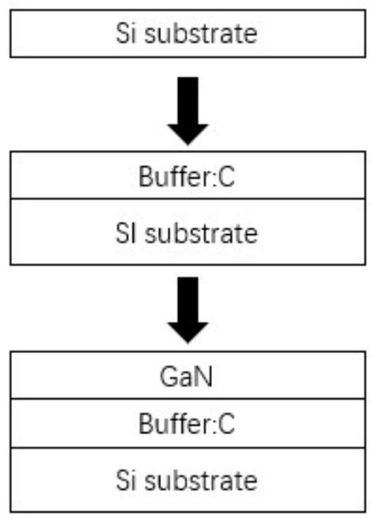
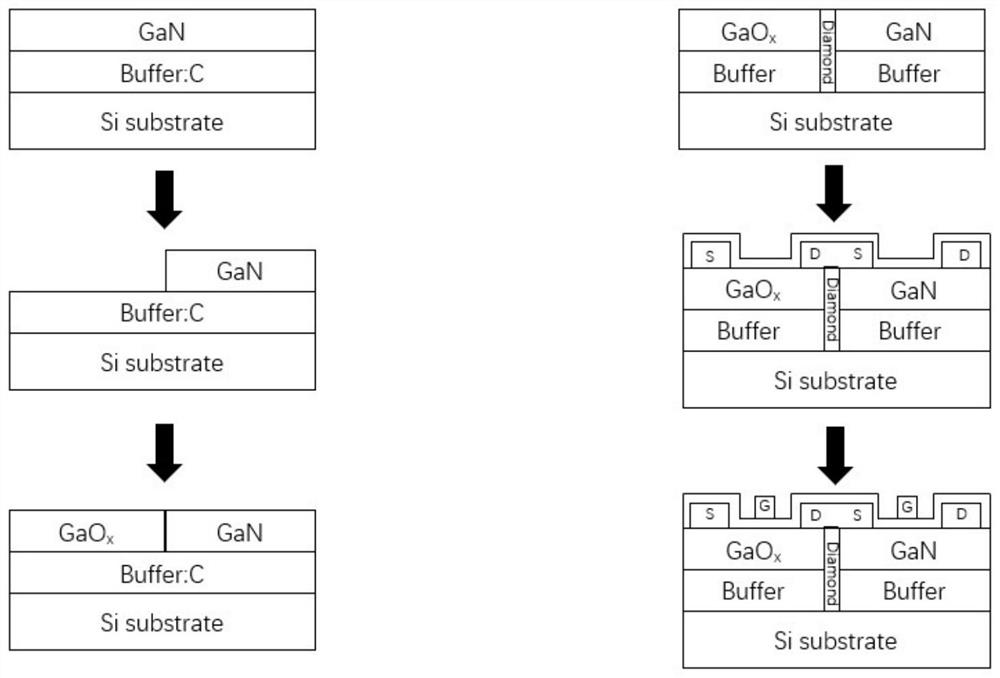
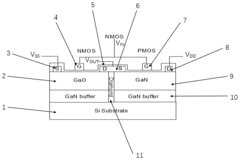
[0024] An embodiment of the present invention provides a GaO-based x -The preparation method of the CMOS inverter of NMOS / GaN-PMOS, comprises the following steps:

[0025] Step 1: Grow a carbon-doped GaN buffer layer on a single crystal Si substrate, block the area on one side of the carbon-doped GaN buffer layer with photoresist, and epitaxially grow Si-GaN on the surface of the carbon-doped GaN buffer layer to form p-MOS The channel layer is etched in part of the surface of the n-MOS channel layer until the carbon-doped GaN buffer layer, using SiO 2 Epitaxial growth of Mg-GaO on the exposed carbon-doped GaN buffer layer as a growth mask x forming an n-MOS channel lay...


PUM

PropertyMeasurementUnit
thicknessaaaaaaaaaa
thicknessaaaaaaaaaa
lengthaaaaaaaaaa

Abstract

The invention discloses a preparation method of a CMOS inverter of GaOx-NMOS / GaN-PMOS. The preparation method comprises the following steps: growing a carbon-doped GaN buffer layer on a Si substrate, blocking a region on one side of the carbon-doped GaN buffer layer by using photoresist, epitaxially growing Si-doped GaN on the other side to form a p-MOS channel layer, removing the photoresist on the other side, blocking the surface of the p-MOS channel layer, etching a partial region of the n-MOS channel layer to the carbon-doped GaN buffer layer, and forming a p-MOS channel layer on the surface of the n-MOS channel layer; growing GaN on the carbon-doped GaN buffer layer exposed after etching by using SiO2 as a growth mask to form a p-MOS channel layer, and epitaxially growing GaOx on the surface of which the photoresist is removed to form an n-MOS channel layer; performing vertical photoetching at critical positions of the n-MOS channel layer and the p-MOS channel layer, and growing diamond in a formed isolation region to form a barrier layer; blocking by using photoresist, and respectively injecting Si and Mg into the surfaces of the n-MOS channel layer and the p-MOS channel layer to form an n region and a p region; and depositing a metal film and a dielectric layer on the surface of the device, stripping, annealing, obtaining a drain electrode and a source electrode in two end regions of the n-MOS channel layer and the p-MOS channel layer in the barrier layer region, and forming grid electrodes in the n-MOS channel layer and the p-MOS channel layer.

Description

technical field [0001] The embodiments of the present invention relate to the technical field of materials, especially a GaO-based x -The preparation method of the CMOS inverter of NMOS / GaN-PMOS. Background technique [0002] In recent years, GaN and Ga 2 O 3 Identified as one of the most important semiconductors for power applications, they all have relatively large band gaps and breakdown electric fields, enabling high voltage, high current, and stable device operation. Inverters with GaN / AlGaN heterojunctions have attracted great attention and are widely used because of their excellent performance. The main features of this type of inverter are: high switching speed, small parasitic inductance; High pressure and other places. [0003] However, the existing inverters have high power consumption, complex fabrication processes, complicated circuits, poor heat dissipation, and the maximum on-current density is limited to several tens of mA / mm. The size of the device is re...

Claims


Application Information

Patent Timeline
Patent Type & Authority Applications(China)
IPC IPC(8): H01L21/8258H01L27/092
CPCH01L21/8258H01L27/092
Inventor 刘新科黄正李博蒋忠伟马正蓊陈增发黄双武朱德亮黎晓华徐平
Owner SHENZHEN UNIV
Learn More