Stable white light OLED (Organic Light Emitting Diode) of multi-light-emitting-layer mixed parent structure without transmission layer
A technology of light-emitting layer and transmission layer, applied in the field of stable white light OLED, can solve the problems of reducing the luminous efficiency and spectral stability of the device, increasing the difficulty of carrier transmission, and increasing the difficulty of manufacturing, so as to avoid excessive turn-on voltage, Increase the coverage and the effect of small CIE coordinate offset
- Summary
- Abstract
- Description
- Claims
- Application Information
AI Technical Summary
Problems solved by technology
Method used
Image
Examples
Embodiment 1
[0036] The preparation of a stable white light OLED with a mixed matrix structure of multiple light-emitting layers without the transport layer includes the following steps:
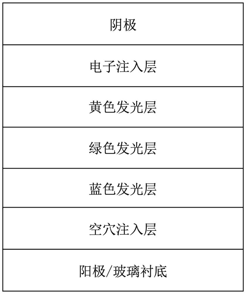
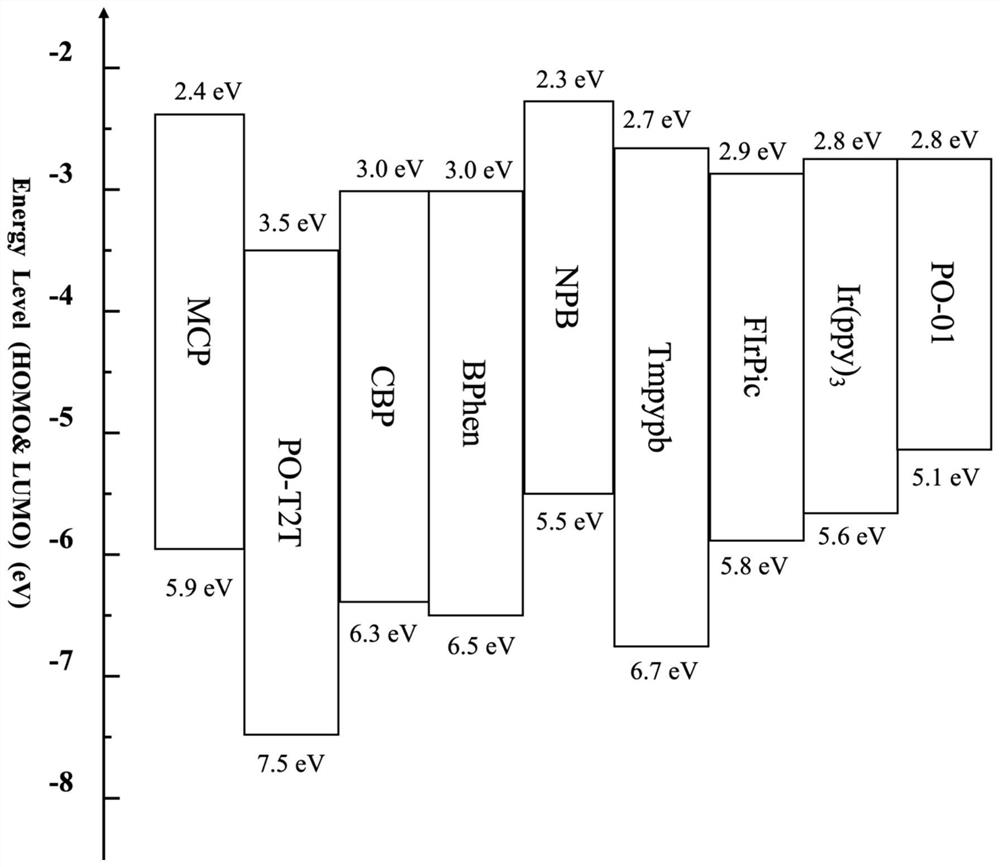
[0037] (1) The device structure is: ITO / MoO 3 (2nm) / MCP:PO-T2T:8wt%FIrPic(25nm) / CBP:BPhen:Ir(ppy) 3 (2:1, 8wt%, 25nm) / TCTA:BCP:8wt%PO-01(25nm) / Liq(1nm) / Al.
[0038] (2) Use acetone, ethanol, and deionized water to repeatedly clean the front and back sides of the ITO glass substrate for 10 minutes, followed by ultrasonic treatment in each of the above three solutions for 10 minutes in turn. The purpose is to remove dust and stains on the glass substrate. Then, the ITO glass substrate was taken out and dried, and then subjected to ultraviolet treatment for 10 min, in order to improve the surface work function of ITO.
[0039] (3) The treated ITO substrate is placed in a multi-source organic molecular vapor deposition system for evaporation, and the organic materials and metal materials used are placed i...
Embodiment 2
[0045] The preparation of a stable white light OLED with a mixed matrix structure of multiple light-emitting layers without the transport layer includes the following steps:
[0046] (1) The device structure is: ITO / MoO 3 (2nm) / MCP:PO-T2T:8wt%FIrPic(25nm) / CBP:BPhen:Ir(ppy) 3 (2:1,8wt%,25nm) / TCTA:BCP:PO-01(1:2,8wt%,25nm) / NPB:TmPyPB:8wt%Ir(piq) 2 (acac)(25nm) / Liq(1nm) / Al.
[0047] (2) Use acetone, ethanol, and deionized water to repeatedly clean the front and back sides of the ITO glass substrate for 10 minutes, followed by ultrasonic treatment in each of the above three solutions for 10 minutes in turn. The purpose is to remove dust and stains on the glass substrate. Then, the ITO glass substrate was taken out and dried, and then subjected to ultraviolet treatment for 10 min, in order to improve the surface work function of ITO.
[0048] (3) The treated ITO substrate is placed in a multi-source organic molecular vapor deposition system for evaporation, and the organic mater...
PUM
| Property | Measurement | Unit |
|---|---|---|
| Thickness | aaaaa | aaaaa |
Abstract
Description
Claims
Application Information


