Supercharge Your Innovation With Domain-Expert AI Agents!

Manufacturing method of InSb focal plane detector and InSb focal plane detector

A focal plane detector and detector chip technology, which is applied in semiconductor devices, radiation control devices, final product manufacturing, etc., can solve the problems of low efficiency, high cost, limited filling factor and radius of curvature, etc., and achieve high filling rate , high production efficiency and small coupling stress

Pending Publication Date: 2022-07-12
11TH RES INST OF CHINA ELECTRONICS TECH GROUP CORP
View PDF0 Cites 0 Cited by
  • Summary
  • Abstract
  • Description
  • Claims
  • Application Information

AI Technical Summary

Problems solved by technology

The existing manufacturing methods mainly include the following: mechanical, micro-nano processing technology, high precision but low efficiency and high cost; the fill factor and radius of curvature of microlenses such as lithography thermal reflow, droplet inkjet, etc. are limited; There are problems such as uniformity, lens curvature, and integration accuracy in transfer printing and other methods

Method used


Image

  • Manufacturing method of InSb focal plane detector and InSb focal plane detector
  • Manufacturing method of InSb focal plane detector and InSb focal plane detector
  • Manufacturing method of InSb focal plane detector and InSb focal plane detector

Examples


Embodiment Construction

[0023] In order to make the purposes, technical solutions and advantages of the embodiments of the present invention clearer, the technical solutions in the embodiments of the present invention will be clearly and completely described below with reference to the accompanying drawings in the embodiments of the present invention. Obviously, the described embodiments These are some embodiments of the present invention, but not all embodiments. Based on the embodiments of the present invention, all other embodiments obtained by those of ordinary skill in the art without creative work fall within the protection scope of the present invention.

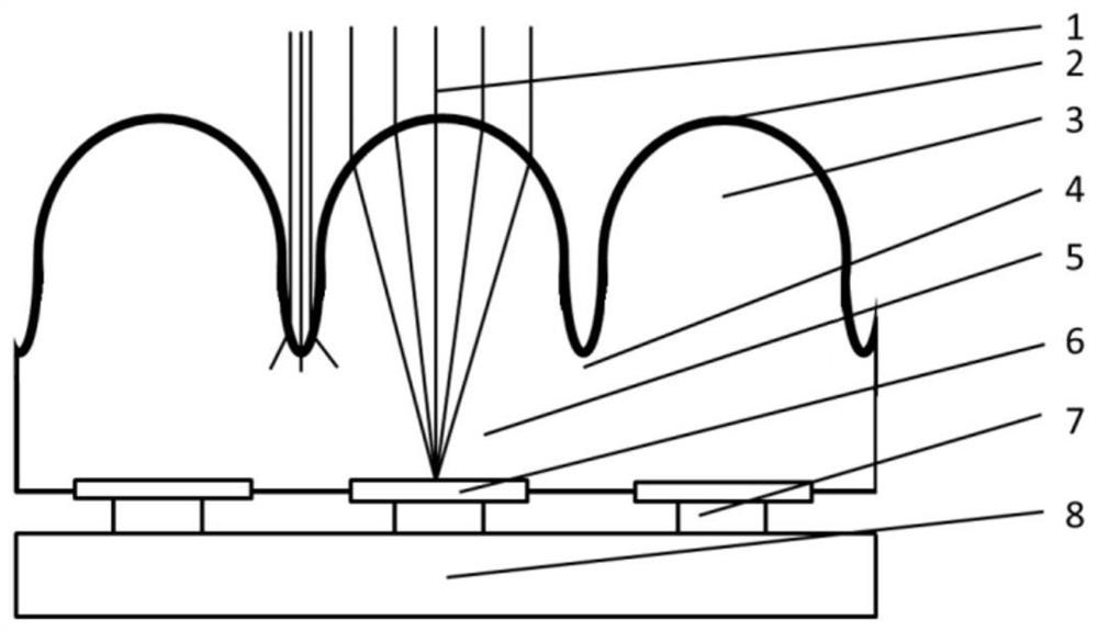
[0024] figure 1 A method for fabricating an InSb focal plane detector provided in an embodiment of the present invention includes: thinning the backside of the InSb detector chip 5 to a preset lens design thickness, and adjusting the backside of the InSb detector chip 5 Surface treatment is performed; the back of the InSb detector chip 5 is...


PUM


Abstract

The invention relates to a manufacturing method of an InSb focal plane detector and the InSb focal plane detector, and the method comprises the steps: thinning the back surface of an InSb detector chip to a preset lens design thickness, and carrying out the surface treatment of the back surface of the InSb detector chip; etching the back surface of the InSb detector chip to form a concave lens and a convex lens; reflecting films are arranged on the sides, away from the InSb detector chip, of the concave lens and the convex lens to form the micro-lens array, the manufacturing efficiency is high, the coupling stress with a detector material is small, the coupling precision is high, and the concave lens and the convex lens are arranged at the same time, so that the overall filling rate of the micro-lens array is high.

Description

technical field [0001] The invention relates to the field of fabrication of microlens arrays, in particular to a fabrication method of an InSb focal plane detector and an InSb focal plane detector. Background technique [0002] The InSb focal plane infrared detector is an infrared detector that works in the mid-wave band, and detects infrared light through the photovoltaic effect of the PN junction. There are usually two types: mesa type and planar type. Arrayed PN junctions are realized by preparing independent mesa structures or arrayed injection regions respectively, and integrated with readout circuits to realize multi-pixel imaging. The isolation structure between the pixel arrays is used for optical and electrical isolation between different photosensitive elements, but it limits the area and filling rate of the PN junction region, thereby limiting its quantum efficiency, and there is a problem of crosstalk. Coupling a microlens array on the surface of the InSb infrar...

Claims


Application Information

Patent Timeline
Patent Type & Authority Applications(China)
IPC IPC(8): H01L27/146H01L31/18H01L31/0232H01L31/101
CPCH01L27/14683H01L27/14685H01L27/14627H01L31/184H01L31/101H01L31/02327Y02P70/50
Inventor 谭启广张轶
Owner 11TH RES INST OF CHINA ELECTRONICS TECH GROUP CORP
Features
  • R&D
  • Intellectual Property
  • Life Sciences
  • Materials
  • Tech Scout
  • Unparalleled Data Quality
  • Higher Quality Content
  • 60% Fewer Hallucinations
Learn More