Eureka AIR delivers breakthrough ideas for toughest innovation challenges, trusted by R&D personnel around the world.

Monocrystalline silicon furnace for processing semiconductor raw material wafer

A semiconductor and raw material technology, applied in the direction of single crystal growth, single crystal growth, crystal growth, etc., can solve the problems of easy shaking, damage, and parts collision, so as to avoid collision and damage, reduce working noise, and prevent heat churn effect

Pending Publication Date: 2022-07-22
赵董生
View PDF0 Cites 0 Cited by
  • Summary
  • Abstract
  • Description
  • Claims
  • Application Information

AI Technical Summary

Problems solved by technology

Due to structural design reasons, the current monocrystalline silicon furnaces on the market lack automatic pressure relief measures. After working for a long time, the internal air pressure is often too large. When the silicon furnace is used for the production and processing of single crystal silicon by the Czochralski method, the crucible is prone to shaking after rotation, so that there will be an offset between the center of the single crystal silicon melt in the crucible and the seed crystal, thereby affecting the quality of the single crystal silicon. The quality of the finished product. In addition, the existing monocrystalline silicon furnace is prone to large vibrations during the working process, which will not only make a huge noise, but also cause the parts in the furnace to collide and be damaged due to vibration.

Method used


Image

  • Monocrystalline silicon furnace for processing semiconductor raw material wafer
  • Monocrystalline silicon furnace for processing semiconductor raw material wafer
  • Monocrystalline silicon furnace for processing semiconductor raw material wafer

Examples


Embodiment Construction

[0025] The technical solutions in the embodiments of the present invention will be clearly and completely described below with reference to the accompanying drawings in the embodiments of the present invention. Obviously, the described embodiments are only a part of the embodiments of the present invention, but not all of the embodiments. Based on the embodiments of the present invention, all other embodiments obtained by those of ordinary skill in the art without creative efforts shall fall within the protection scope of the present invention.

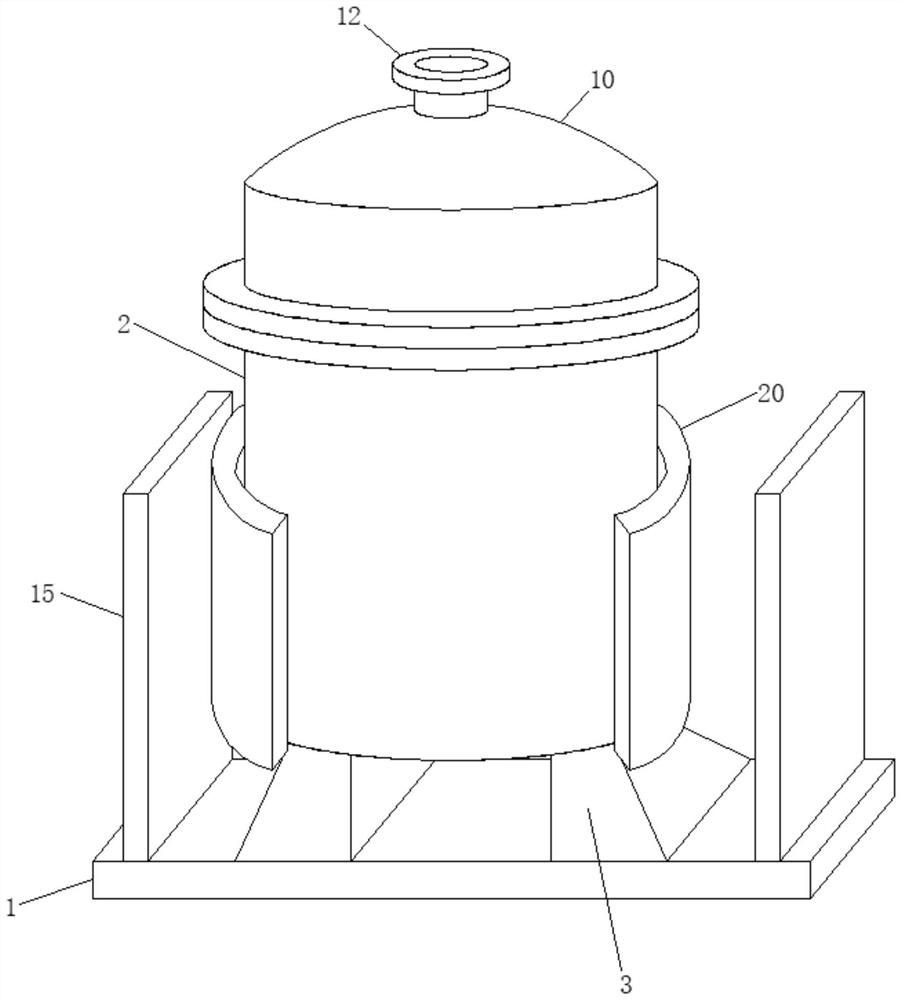
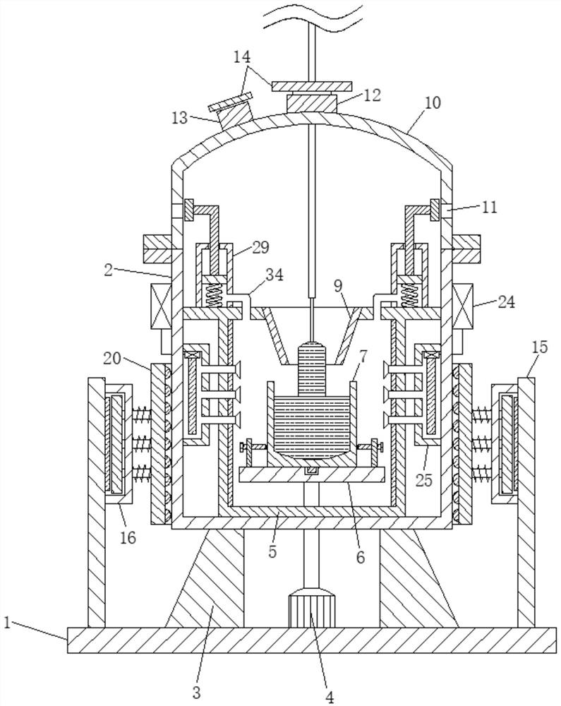
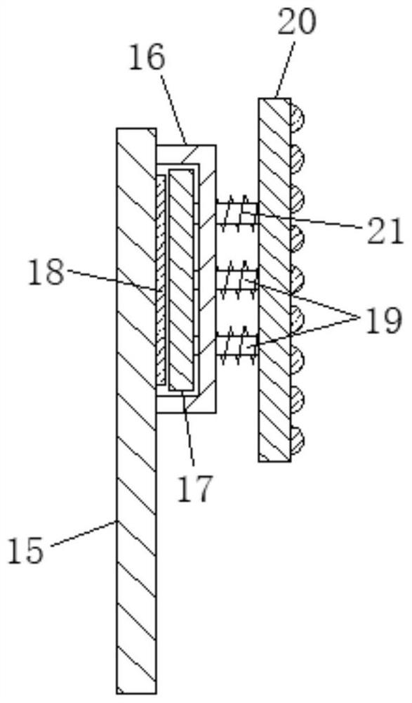
[0026] see Figure 1-7, the present invention provides a technical solution: a single crystal silicon furnace for semiconductor raw material wafer processing, comprising a base 1, a furnace body 2 is arranged above the base 1, the cross-section of the furnace body 2 is circular, and the bottom of the furnace body 2 is circular. A number of supporting feet 3 are fixedly connected, and the supporting feet 3 are fixedly connected to the ...


PUM


Abstract

The invention relates to a monocrystalline silicon furnace for semiconductor raw material wafer processing, which comprises a base, a furnace body is arranged above the base, damping mechanisms are arranged on both sides of the furnace body, a motor is arranged below the furnace body, the inner wall of the furnace body is fixedly connected with a heat preservation cylinder, and the top end of an output shaft of the motor penetrates through the bottom of the furnace body and is fixedly connected with a turntable; and heating mechanisms are arranged on the two sides of the heat preservation cylinder, pressure relief mechanisms are arranged on the two sides of the top of the heat preservation cylinder, and a furnace cover is installed on the top of the furnace body. According to the single crystal silicon furnace, automatic pressure relief can be achieved to guarantee air pressure balance in the heat preservation barrel, potential safety hazards caused by too large air pressure in the heat preservation barrel are avoided, the quartz crucible can be limited so that the stability of the quartz crucible can be improved, in addition, the damping effect on the furnace body can be achieved so that the working noise of the single crystal silicon furnace can be reduced, and the service life of the single crystal silicon furnace can be prolonged. And meanwhile, parts in the furnace body are effectively prevented from being damaged due to collision caused by vibration.

Description

technical field [0001] The invention relates to the technical field of semiconductors, in particular to a single crystal silicon furnace used for processing semiconductor raw material wafers. Background technique [0002] Wafer refers to the silicon wafer used to make silicon semiconductor circuits, and its raw material is silicon. High-purity polysilicon is dissolved and mixed with silicon crystal seeds, which are then slowly pulled out to form cylindrical monocrystalline silicon. The silicon ingot is ground, polished and sliced ​​to form a silicon wafer, that is, a wafer. [0003] A single crystal silicon furnace is a manufacturing equipment for producing single crystal silicon by the Czochralski method. Most of the wafer production and processing are completed by a single crystal silicon furnace. Due to the structural design of the current monocrystalline silicon furnaces on the market, there is a lack of automatic pressure relief measures. When working for a long time,...

Claims


Application Information

Patent Timeline
Patent Type & Authority Applications(China)
IPC IPC(8): C30B15/00C30B15/10C30B29/06
CPCC30B15/00C30B15/10C30B29/06
Inventor 赵董生
Owner 赵董生
Why Eureka
Eureka Blog
Learn More