Neuromorphic visual sensor and application and preparation method thereof
A visual sensor, neuromorphic technology, applied in semiconductor/solid-state device manufacturing, semiconductor devices, electric solid-state devices, etc., to achieve high-efficiency sensing functions, improve processing speed and computing efficiency
- Summary
- Abstract
- Description
- Claims
- Application Information
AI Technical Summary
Problems solved by technology
Method used
Image

Examples
Embodiment 1
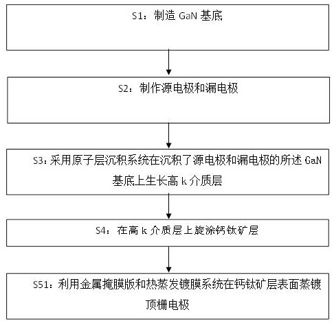
[0044] The embodiment of the present invention provides a preparation method of a neuromorphic vision sensor based on a perovskite hetero-gate structure, see figure 1 and figure 2 , which includes the following steps:
[0045] The first step is to fabricate a GaN substrate.
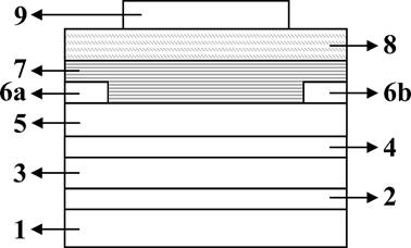
[0046] like figure 1 As shown, in the embodiment of the present invention, a metal chemical vapor deposition system is used to grow a high-quality AlGaN / GaN heterojunction material on the SiC substrate 1, and the heterojunction material is an epitaxial layer structure. AlN nucleation layer 2 , GaN buffer layer 3 , AlN insertion layer 4 , and AlGaN barrier layer 5 .
[0047] Preferably, the thickness of the AlN nucleation layer 2 is 100 nm, the thickness of the GaN buffer layer 3 is 1.5 μm, the thickness of the AlN insertion layer 4 is 1 nm, and the thickness of the AlGaN barrier layer 5 is 22 nm.
[0048] In step 2, the source electrode 6a and the drain electrode 6b are fabricated.
[0049] Specific...
Embodiment 2
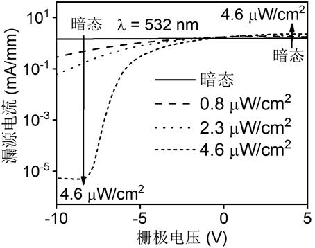
[0069] This embodiment provides a neuromorphic vision sensor based on a perovskite hetero-gate structure, which is prepared according to the preparation method provided in the first embodiment. Figures 3 to 8 The performance test results of the neuromorphic vision sensor based on the perovskite hetero-gate structure are shown.
[0070] see image 3 , image 3 Shown is the perovskite hetero-gate structure-based neuromorphic vision sensor at drain-source bias V ds =1 V, when the incident light is 532 nm, the transfer characteristic curves measured under different laser power densities, different laser power densities ( image 3 arrow direction) including 0.8µW / cm 2 , 2.3µW / cm 2 , 4.6µW / cm 2 . in, image 3 The abscissa is the gate voltage V gs , the ordinate is the drain-source current I ds . from image 3 It can be seen in the 532nm light stimulation that even if the incident light power is very small, the transfer characteristic curve will still change, that is, the...
PUM
| Property | Measurement | Unit |
|---|---|---|
| thickness | aaaaa | aaaaa |
| thickness | aaaaa | aaaaa |
| thickness | aaaaa | aaaaa |
Abstract
Description
Claims
Application Information
 - R&D
- Intellectual Property
- Life Sciences
- Materials
- Tech Scout
- Unparalleled Data Quality
- Higher Quality Content
- 60% Fewer Hallucinations
Browse by: Latest US Patents, China's latest patents, Technical Efficacy Thesaurus, Application Domain, Technology Topic, Popular Technical Reports.
© 2025 PatSnap. All rights reserved.Legal|Privacy policy|Modern Slavery Act Transparency Statement|Sitemap|About US| Contact US: help@patsnap.com