
Patsnap Eureka
For R&D, Patsnap Eureka makes reading and utilizing patents & technical documents easy.
Patsnap Eureka AIR
Designed for self-driven R&D workflows. Generate viable solutions, solve complex R&D challenges, empower your innovation with AI.

Patsnap Eureka Materials
Designed for material experts only. Revolutionize your material R&D, from search, analyze, to developing new materials.

TechResearch
Generate reliable direction feasibility study reports for your R&D in just a few steps.

TechSeek
Discover and master advanced knowledge NOW. Basics, ideas, possibilities, all at once.

TechMind
As an expert in R&D Theories, TechMind can generates customized viable solutions instantly.

TechRisk
Analyze your overall solution with one click, know your potential R&D risks in advance.

TechMonitor
Get weekly tech updates, stay abreast of the latest tech innovations and key insights.
Semiconductor device and preparation method thereof
A semiconductor and device technology, applied in the field of semiconductor devices and their preparation, can solve problems such as cumbersome process, lattice mismatch, GaN epitaxial film cracks, etc., and achieve the effect of ensuring growth quality and reducing the risk of leakage
- Summary
- Abstract
- Description
- Claims
- Application Information
AI Technical Summary
Problems solved by technology
Method used
Image

Examples
Embodiment Construction
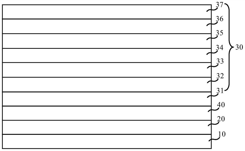
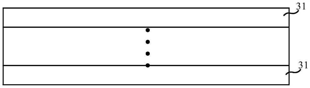
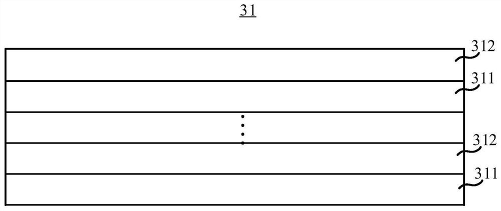
[0040] The technical solutions in the embodiments of the present application will be clearly and completely described below with reference to the drawings in the embodiments of the present application. Obviously, the described embodiments are only a part of the embodiments of the present application, but not all of the embodiments. Based on the embodiments in this application, all other embodiments obtained by those skilled in the art without creative efforts shall fall within the protection scope of this application. In addition, it should be understood that the specific embodiments described herein are only used to illustrate and explain the present application, but not to limit the present application. In this application, unless otherwise stated, the directional words used such as "up", "down", "left" and "right" usually refer to the upper, lower and left of the device in actual use or working state. and right, specifically the direction of the drawing in the drawings.
...
PUM
| Property | Measurement | Unit |
|---|---|---|
| thickness | aaaaa | aaaaa |
| thickness | aaaaa | aaaaa |
Abstract
Description
Claims
Application Information
 - R&D Engineer
- R&D Manager
- IP Professional
- Industry Leading Data Capabilities
- Powerful AI technology
- Patent DNA Extraction
Browse by: Latest US Patents, China's latest patents, Technical Efficacy Thesaurus, Application Domain, Technology Topic, Popular Technical Reports.
© 2024 PatSnap. All rights reserved.Legal|Privacy policy|Modern Slavery Act Transparency Statement|Sitemap|About US| Contact US: help@patsnap.com